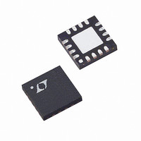
LT5512EUF Linear Technology, LT5512EUF Datasheet - Page 8

LT5512EUF
Manufacturer Part Number
LT5512EUF
Description
IC MIXER DWNCONV HI SIGN 16-QFN
Manufacturer
Linear Technology
Series
LT5512r
Datasheet
1.LT5512EUF.pdf
(12 pages)
Specifications of LT5512EUF
Rf Type
Cellular, HF, ISM, PCS, UHF, VHF, WMTS
Frequency
1kHz ~ 3GHz
Number Of Mixers
1
Gain
1.1dB
Noise Figure
14dB
Secondary Attributes
Down Converter
Current - Supply
74mA
Voltage - Supply
4.5 V ~ 5.25 V
Package / Case
16-WQFN Exposed Pad
Operating Temperature (min)
-40C
Operating Temperature (max)
85C
Operating Temperature Classification
Industrial
Lead Free Status / RoHS Status
Contains lead / RoHS non-compliant
Available stocks
Company
Part Number
Manufacturer
Quantity
Price
Part Number:
LT5512EUF
Manufacturer:
LINEAR/凌特
Quantity:
20 000
Part Number:
LT5512EUF#PBF
Manufacturer:
LINEAR/凌特
Quantity:
20 000
Company:
Part Number:
LT5512EUF#TRPBF
Manufacturer:
SP
Quantity:
5 997
Part Number:
LT5512EUF#TRPBF
Manufacturer:
LINEAR/凌特
Quantity:
20 000
APPLICATIO S I FOR ATIO
LT5512
The LT5512 consists of a double-balanced mixer, RF buffer
amplifi er, high-speed limiting LO buffer and bias/enable
circuits. The differential RF, LO and IF ports require simple
external matching which allows the mixer to be used at
very low frequencies, below 1MHz, or up to 3GHz. Low
side or high side LO injection can be used.
Two evaluation circuits are available. The HF/VHF/UHF
evaluation circuit is shown in Figure 1 and the 900MHz
to 2.5GHz evaluation circuit is shown in Figure 2. The
corresponding demo board layouts are shown in Figures
10 and 11, respectively.
RF Input Port
A simplifi ed schematic of the differential RF input is
shown in Figure 3, with the associated external imped-
ance matching elements for a 450MHz application. Each
RF input requires a low resistance DC return to ground
8
50Ω
Figure 3. RF Input with External Matching
RS
Figure 4. 450MHz RF Input Matching
LT5512
15mA
4.7nH
C4
L1
for a 450MHz Application
RF
50Ω
U
2
IN
L1
L2
U
10pF
V
1:1
C4
CC
2
3
1/2 X
1/2 X
W
3
j2.6
j2.6
INT
INT
L2
4.7nH
15mA
V
BIAS
LT5512
5512 F03
RL
18.1Ω
5512 F04
U
capable of sinking 15mA. This can be accomplished with
the center-tap of a balun as shown in Figure 3, or with
bias chokes connected from Pins 2 and 3 to ground, if a
differential RF input signal is available. The value of the
bias chokes should be high enough to avoid reducing the
input impedance at the frequency of interest.
Table 1 lists the differential input impedance and differen-
tial refl ection coeffi cient between Pins 2 and 3 for several
common RF frequencies. As shown in Figures 3 and 4,
low-pass impedance matching is used to transform the
differential input impedance up to the desired value for
the balun input. The following example shows how to
design the low-pass impedance transformation network
for the RF input.
From Table 1, the differential input impedance at 450MHz
is 18.1 + j5.2. As shown in Figure 4, the 5.2Ω reactance is
split, with one half on each side of the 18.1Ω load resistor.
The matching network will consist of additional inductance
in series with the internal inductance and a capacitor in
parallel with the desired 50Ω source impedance. The ca-
pacitance (C4) and inductance are calculated as follows.
Table 1. RF Input Differential Impedance
L L
Q
C
1 2
4
,
=
=
=
Frequency
4 2
ω
(
(MHz)
=
1900
2150
2450
2700
R
.
240
450
950
Q
R
10
44
S
R
nH use
S
/
L
2
=
R
ω
•
(
L
2
Q
) –
π π
=
•
1
4 7
450
2 2
Differential Input
=
1 328
.
•
1 1 8 1 1 328
.
18.2 + j0.14
18.7 + j11.3
20.6 + j22.8
21.4 + j26.5
22.5 + j30.5
24.1 + j34.7
Impedance
18.1 + j2.8
18.1 + j5.2
nH
18 + j0.26
MHz
π
(
. • .
50 18 1 1 1 328
) )
•
450
/
•
50
MHz
. ) –
=
9 4
.
0.467
0.470
0.471
0.473
0.479
0.503
0.512
0.522
0.530
Mag
=
pF use
Differential S11
.
(
10
Angle
179.6
178.6
172.6
166.3
150.8
124.3
116.9
109.2
101.7
pF
5512fa
)


