SI4311-B10-GM Silicon Laboratories Inc, SI4311-B10-GM Datasheet - Page 18
SI4311-B10-GM
Manufacturer Part Number
SI4311-B10-GM
Description
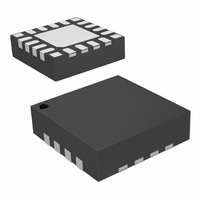
IC RX FSK 315/434MHZ 20VQFN
Manufacturer
Silicon Laboratories Inc
Series
EZRadio®r
Type
ISM Receiverr
Datasheets
1.SI4311-B10-GM.pdf
(20 pages)
2.SI4311-B10-GM.pdf
(2 pages)
3.SI4311-B10-GM.pdf
(20 pages)
Specifications of SI4311-B10-GM
Package / Case
20-VQFN
Frequency
315MHz, 434MHz
Sensitivity
-104dBm
Data Rate - Maximum
10 kBaud
Modulation Or Protocol
FSK
Applications
Garage Openers, RKE, Security Alarms
Data Interface
PCB, Surface Mount
Antenna Connector
PCB, Surface Mount
Voltage - Supply
2.7 V ~ 3.6 V
Operating Temperature
-40°C ~ 85°C
Operating Frequency
315 MHz to 434 MHz
Operating Supply Voltage
2.7 V to 3.6 V
Maximum Operating Temperature
+ 95 C
Minimum Operating Temperature
- 45 C
Mounting Style
SMD/SMT
Supply Current
20 mA
Lead Free Status / RoHS Status
Lead free / RoHS Compliant
Features
-
Memory Size
-
Current - Receiving
-
Lead Free Status / Rohs Status
Lead free / RoHS Compliant
Other names
336-1976-5


Si 4311
18
Notes:
General
Solder Mask Design
Stencil Design
Card Assembly
Symbol
1. All dimensions shown are in millimeters (mm) unless otherwise noted.
2. Dimensioning and tolerancing is per the ANSI Y14.5M-1994 specification.
3. This land pattern design is based on IPC-SM-782 guidelines.
4. All dimensions shown are at Maximum Material Condition (MMC). Least Material
5. All metal pads are to be non-solder-mask-defined (NSMD). Clearance between the
6. A stainless steel, laser-cut and electro-polished stencil with trapezoidal walls should
7. The stencil thickness should be 0.125 mm (5 mils).
8. The ratio of stencil aperture to land pad size should be 1:1 for the perimeter pads.
9. A 1.45 x 1.45 mm square aperture should be used for the center pad. This provides
10. A No-Clean, Type-3 solder paste is recommended.
11. The recommended card reflow profile is per the JEDEC/IPC J-STD-020 specification
GD
D2
E2
D
E
e
f
Condition (LMC) is calculated based on a fabrication allowance of 0.05 mm.
solder mask and the metal pad is to be 60 µm minimum, all the way around the pad.
be used to assure good solder paste release.
approximately 70% solder paste coverage on the pad, which is optimum to assure
correct component standoff.
for small body components.
1.60
1.60
2.10
Min
Table 13. PCB Land Pattern Dimensions
Millimeters
2.71 REF
0.50 BSC
2.71 REF
2.53 BSC
Max
1.80
1.80
—
Rev. 0.5
Symbol
GE
ZD
ZE
W
X
Y
2.10
Min
—
—
—
—
Millimeters
0.61 REF
Max
0.34
0.28
3.31
3.31
—
Related parts for SI4311-B10-GM
Image
Part Number
Description
Manufacturer
Datasheet
Request
R

Part Number:
Description:
SI4311-B11-GM
Manufacturer:
Silicon Laboratories Inc
Datasheet:
Part Number:
Description:
QFN 20/I°/315/434 MHZ FSK RECEIVER
Manufacturer:
Silicon Laboratories Inc
Part Number:
Description:
SMD/C°/SINGLE-ENDED OUTPUT SILICON OSCILLATOR
Manufacturer:
Silicon Laboratories Inc
Part Number:
Description:
Manufacturer:
Silicon Laboratories Inc
Datasheet:
Part Number:
Description:
N/A N/A/SI4010 AES KEYFOB DEMO WITH LCD RX
Manufacturer:
Silicon Laboratories Inc
Datasheet:
Part Number:
Description:
N/A N/A/SI4010 SIMPLIFIED KEY FOB DEMO WITH LED RX
Manufacturer:
Silicon Laboratories Inc
Datasheet:
Part Number:
Description:
N/A/-40 TO 85 OC/EZLINK MODULE; F930/4432 HIGH BAND (REV E/B1)
Manufacturer:
Silicon Laboratories Inc
Part Number:
Description:
EZLink Module; F930/4432 Low Band (rev e/B1)
Manufacturer:
Silicon Laboratories Inc
Part Number:
Description:
I°/4460 10 DBM RADIO TEST CARD 434 MHZ
Manufacturer:
Silicon Laboratories Inc
Part Number:
Description:
I°/4461 14 DBM RADIO TEST CARD 868 MHZ
Manufacturer:
Silicon Laboratories Inc
Part Number:
Description:
I°/4463 20 DBM RFSWITCH RADIO TEST CARD 460 MHZ
Manufacturer:
Silicon Laboratories Inc
Part Number:
Description:
I°/4463 20 DBM RADIO TEST CARD 868 MHZ
Manufacturer:
Silicon Laboratories Inc
Part Number:
Description:
I°/4463 27 DBM RADIO TEST CARD 868 MHZ
Manufacturer:
Silicon Laboratories Inc
Part Number:
Description:
I°/4463 SKYWORKS 30 DBM RADIO TEST CARD 915 MHZ
Manufacturer:
Silicon Laboratories Inc