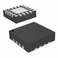
SI4311-B10-GM Silicon Laboratories Inc, SI4311-B10-GM Datasheet - Page 9

SI4311-B10-GM
Manufacturer Part Number
SI4311-B10-GM
Description
IC RX FSK 315/434MHZ 20VQFN
Manufacturer
Silicon Laboratories Inc
Series
EZRadio®r
Type
ISM Receiverr
Datasheets
1.SI4311-B10-GM.pdf
(20 pages)
2.SI4311-B10-GM.pdf
(2 pages)
3.SI4311-B10-GM.pdf
(20 pages)
Specifications of SI4311-B10-GM
Package / Case
20-VQFN
Frequency
315MHz, 434MHz
Sensitivity
-104dBm
Data Rate - Maximum
10 kBaud
Modulation Or Protocol
FSK
Applications
Garage Openers, RKE, Security Alarms
Data Interface
PCB, Surface Mount
Antenna Connector
PCB, Surface Mount
Voltage - Supply
2.7 V ~ 3.6 V
Operating Temperature
-40°C ~ 85°C
Operating Frequency
315 MHz to 434 MHz
Operating Supply Voltage
2.7 V to 3.6 V
Maximum Operating Temperature
+ 95 C
Minimum Operating Temperature
- 45 C
Mounting Style
SMD/SMT
Supply Current
20 mA
Lead Free Status / RoHS Status
Lead free / RoHS Compliant
Features
-
Memory Size
-
Current - Receiving
-
Lead Free Status / Rohs Status
Lead free / RoHS Compliant
Other names
336-1976-5
3. Functional Description
3.1. Overview
The Si4311 is a fully-integrated FSK CMOS RF receiver
that operates in the unlicensed 315 and 433.92 MHz
ultra high frequency (UHF) bands. It is designed for
high-volume, cost-sensitive RF receiver applications.
The chip operates at a carrier frequency of 315 or
433.92 MHz and supports FSK digital modulation with
data rates of up to 10 kbps.
The device leverages Silicon Labs’ patented and proven
digital low-IF architecture and offers superior sensitivity
and interference rejection. The Si4311 can achieve
superior sensitivity in the presence of large interference
due to its high dynamic range ADCs and digital filters.
The digital low-IF architecture also enables superior
blocking ability and low intermodulation distortion for
robust reception in the presence of wide-band
interference.
Digital integration reduces the number of required
external components compared to traditional offerings,
resulting in a solution that only requires a 16 MHz
crystal and passive components allowing a small and
compact printed circuit board (PCB) implementation
area. The high integration of the Si4311 improves the
system manufacturing reliability, improves quality, eases
design-in, and minimizes costs.
2.7 – 3.6 V
Antenna
RX_IN
VDD
GND
LNA
AGC
LDO
Figure 3. Functional Block Diagram
Rev. 0.5
PGA
AFC
3.2. Receiver Description
The RF input signal is amplified by a low-noise amplifier
(LNA) and down-converts to a low intermediate
frequency with a quadrature image-reject mixer. The
mixer output is amplified by a programmable gain
amplifier (PGA), filtered, and digitized with a high-
resolution analog-to-digital converter (ADC). All RF
functions are integrated into the device eliminating any
production alignment issues associated with external
components, such as SAW and ceramic IF filters.
Silicon Labs’ advanced digital low-IF architecture
achieves superior performance by using the DSP to
perform channel filtering, demodulation, automatic gain
control (AGC), automatic frequency control (AFC), and
other baseband processing. DSP implementation of the
channel filters provides better repeatability and control
of the bandwidth and frequency response of the filter
compared to analog implementations. No off-chip
ceramic filters are needed with the Si4311 since all IF
channel filtering is performed in the digital domain.
3.3. Carrier Frequency Selection
The Si4311 can be tuned to either 315 or 433.92 MHz
by driving Pin 6 (315/434) to VDD or GND. The
315 MHz operation is chosen by driving Pin 6 (315/434)
to VDD, and 433.92 MHz operation is chosen by driving
Pin 6 (315/434) to GND.
16 MHz
XTAL
ADC
ADC
OSC
PROCESSOR
BASEBAND
SQUELCH
MCU
DSP
Si4311
DOUT
315/434
DEV[1:0]
BT[1:0]
AFC
RST
Si4311
9


