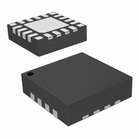
SI4312-B10-GM Silicon Laboratories Inc, SI4312-B10-GM Datasheet - Page 4

SI4312-B10-GM
Manufacturer Part Number
SI4312-B10-GM
Description
IC RX OOK 315/434MHZ 20VQFN
Manufacturer
Silicon Laboratories Inc
Series
EZRadio®r
Type
ISM Receiverr
Specifications of SI4312-B10-GM
Package / Case
20-VQFN
Frequency
315MHz, 434MHz
Sensitivity
-110dBm
Data Rate - Maximum
10 kBaud
Modulation Or Protocol
OOK
Applications
Garage Openers, RKE, Security Alarms
Data Interface
PCB, Surface Mount
Antenna Connector
PCB, Surface Mount
Voltage - Supply
2.7 V ~ 3.6 V
Operating Temperature
-40°C ~ 85°C
Operating Frequency
315 MHz to 434 MHz
Operating Supply Voltage
2.7 V to 3.6 V
Maximum Operating Temperature
+ 95 C
Minimum Operating Temperature
- 45 C
Mounting Style
SMD/SMT
Supply Current
20 mA
Lead Free Status / RoHS Status
Lead free / RoHS Compliant
Features
-
Memory Size
-
Current - Receiving
-
Lead Free Status / Rohs Status
Lead free / RoHS Compliant
Other names
336-1977-5
Si4312
1. Electrical Specifications
Table 1. Recommended Operating Conditions*
Table 2. Absolute Maximum Ratings
4
Parameter
*Note: All minimum and maximum specifications are guaranteed and apply across the recommended operating conditions.
Parameter
Supply Voltage
Input Current
Input Voltage
Operating Temperature
Storage Temperature
RF Input Level
Notes:
Supply Voltage
Supply Voltage Powerup Rise Time
Ambient Temperature
1. Permanent device damage may occur if the absolute maximum ratings are exceeded. Functional operation should be
2. The Si4312 device is a high-performance RF integrated circuit with certain pins having an ESD rating of < 2 kV HBM.
3. For input pins 315/434, RATIO, BT[1:0], TH[1:0].
4. At RF input pin RX_IN.
Typical values apply at V
otherwise stated.
restricted to the conditions as specified in the operational sections of this data sheet. Exposure beyond recommended
operating conditions for extended periods may affect device reliability.
Handling and assembly of this device should only be done at ESD-protected workstations.
3
3
4
DD
= 3.3 V and 25 C unless otherwise stated. Parameters are tested in production unless
1,2
V
Symbol
DD-RISE
V
T
DD
A
Symbol
T
V
T
V
I
STG
OP
DD
IN
IN
Rev. 0.5
Test Condition
–0.3 to (V
–0.5 to 3.9
–55 to 150
–45 to 95
Value
0.4
10
DD
Min
+ 0.3)
2.7
–40
10
Typ
3.3
—
25
Max
3.6
Unit
85
V
—
mA
C
C
V
V
PK
Unit
μs
°C
V


