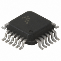
MC33594FTAR2 Freescale Semiconductor, MC33594FTAR2 Datasheet - Page 13

MC33594FTAR2
Manufacturer Part Number
MC33594FTAR2
Description
IC RF RECEIVER 315,434MHZ 24LQFP
Manufacturer
Freescale Semiconductor
Datasheet
1.MC33594FTAR2.pdf
(28 pages)
Specifications of MC33594FTAR2
Frequency
315MHz, 434MHz
Sensitivity
-105dBm
Data Rate - Maximum
11 kBaud
Modulation Or Protocol
FSK, OOK
Applications
General Data Transfer
Current - Receiving
5.7mA
Data Interface
PCB, Surface Mount
Antenna Connector
PCB, Surface Mount
Voltage - Supply
4.5 V ~ 5.5 V
Operating Temperature
-40°C ~ 105°C
Package / Case
24-LQFP
Operating Band Frequency
315 to 434MHz
Operating Frequency (max)
434000kHz
Operating Temperature (min)
-40C
Operating Temperature (max)
105C
Operating Temperature Classification
Industrial
Modulation Type
FSK/OOK
Package Type
LQFP
Product Depth (mm)
4mm
Product Length (mm)
4mm
Operating Supply Voltage (min)
4.5V
Operating Supply Voltage (typ)
5V
Operating Supply Voltage (max)
5.5V
Lead Free Status / RoHS Status
Contains lead / RoHS non-compliant
Features
-
Memory Size
-
Lead Free Status / Rohs Status
Compliant
Other names
MC33594FTAR2TR
Available stocks
Company
Part Number
Manufacturer
Quantity
Price
STATE MACHINES
AFTER POR RESET STATE MACHINE
receiver is enabled. The crystal oscillator is running and generates the clock for the SPI. This implies that before
the circuit is in sleep mode, a delay corresponding to the crystal oscillator wake-up time must be inserted
between the falling edge on RESETB and the start of the transmission on the SPI lines. The local oscillator is
running as well. This means that demodulated data can be read on DMDAT but are not sent by the SPI.
telegram or receiving one.
sampling clock at 615kHz (sampling period Ts=1.6µs), derivated from the crystal oscillator. The transition time
between state 1 and states 2 or 6 is less than 3
use ROMEO2 in a standalone configuration without any external control.
As long as a low level is applied on RESETB, the circuit stays in state 1. This configuration mode enables to write
or read the internal registers through the SPI interface.
© Motorola, Inc., 2002.
There are 3 different modes for the receiver.
Sleep mode corresponds to the low power consumption mode:
Configuration mode is used for writing or reading the internal registers. In this mode, the SPI is slave and the
In Run mode, the receiver is enabled (crystal and local oscillators are running). It is either waiting for an RF
Figure 14 details the state machine after Power On Reset (POR). The state machine is synchronized by a
After POR, the circuit is in state 0 and configuration registers’ content is set to the reset value. This enables to
- if SOE=0, the whole receiver is shutdown,
- if SOE=1, the strobe oscillator remains active.
AND DME=0
RESETB=1
State 2, see figure 15
Freescale Semiconductor, Inc.
AND DME=1
AND SOE=1
Power-On Reset
RESETB=1
For More Information On This Product,
MOTOROLA SEMICONDUCTORS PRODUCTS
Figure 14: After POR state machine
SPI active and slave
Configuration mode
SPI disabled
RESETB=0
Sleep mode
Go to: www.freescale.com
State 0
State 1
×
AND DME=1
Ts.
AND SOE=0
MC33594
RESETB=1
State 6, see figure 16
13
Strobe Counter=SR
Raw data on MOSI
Strobe Counter ≠ SR
OR STROBE=1
AND STROBE=0
SPI disabled
Run mode
State 0b
SPI master
SPI disabled
SPI slave
revision 1.1, 5 February 2002


