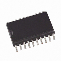
ATA5743P3-TKQY Atmel, ATA5743P3-TKQY Datasheet - Page 11

ATA5743P3-TKQY
Manufacturer Part Number
ATA5743P3-TKQY
Description
IC RCVR ASK/FSK 300KHZ 20SSOP
Manufacturer
Atmel
Datasheet
1.ATA5743P3-TGQY.pdf
(43 pages)
Specifications of ATA5743P3-TKQY
Frequency
300MHz ~ 450MHz
Sensitivity
-110dBm
Data Rate - Maximum
10 kBaud
Modulation Or Protocol
ASK, FSK
Applications
RKE, Telemetering, Security Technology
Current - Receiving
7.5mA
Data Interface
PCB, Surface Mount
Antenna Connector
PCB, Surface Mount
Voltage - Supply
4.5 V ~ 5.5 V
Operating Temperature
-40°C ~ 105°C
Package / Case
20-SOIC (0.200", 5.30mm Width)
Operating Frequency (max)
450000kHz
Operating Temperature (min)
-40C
Operating Temperature (max)
105C
Operating Temperature Classification
Industrial
Product Depth (mm)
4.4mm
Operating Supply Voltage (min)
4.5V
Operating Supply Voltage (typ)
5V
Operating Supply Voltage (max)
5.5V
Lead Free Status / RoHS Status
Lead free / RoHS Compliant
Features
-
Memory Size
-
Lead Free Status / Rohs Status
Compliant
Available stocks
Company
Part Number
Manufacturer
Quantity
Price
Company:
Part Number:
ATA5743P3-TKQY
Manufacturer:
ATMEL
Quantity:
5 000
Part Number:
ATA5743P3-TKQY
Manufacturer:
ATMEL/爱特梅尔
Quantity:
20 000
6.1
4839B–RKE–08/05
Basic Clock Cycle of the Digital Circuitry
The complete timing of the digital circuitry and the analog filtering is derived from one clock. As
seen in
tion with a divider. The division factor is controlled by the logical state at pin MODE. As
described in section
defined by the RF input signal (f
oscillator (f
Figure 6-1.
Pin MODE can now be set in accordance with the desired clock cycle T
following application relevant parameters:
Most applications are dominated by two transmission frequencies: f
used in the USA, f
parameters on these electrical characteristics, here are displayed the three conditions for each
parameter.
The clock cycle of some function blocks depends on the selected baud-rate range (BR_Range)
which is defined in the OPMODE register. This clock cycle T
mulas for further reference:
BR_Range =
• Timing of the polling circuit including bit check
• Timing of the analog and digital signal processing
• Timing of the register programming
• Frequency of the reset marker
• IF filter center frequency (f
• Application USA (f
• Application Europe (f
• Other applications (T
electrical characteristic is given as a function of T
Figure
LO
).
Generation of the Basic Clock Cycle
6-1, this clock cycle T
Send
“RF Front-end” on page
XTO
= 433.92 MHz in Europe. In order to ease the usage of all T
XTO
Clk
= 4.90625 MHz, MODE = L, T
is dependent on f
= 6.76438 MHz, MODE = H, T
IF0
BR_Range0:
BR_Range1:
BR_Range2:
BR_Range3:
)
Divider
:14/:10
RFin
XTO
T
f
CLK
) which also defines the operating frequency of the local
XTO
Clk
is derived from the crystal oscillator (XTO) in combina-
XTO
16
15
14
MODE
DVCC
XTO
5, the frequency of the crystal oscillator (f
and on the logical state of pin MODE. The
Clk
L : USA(:10)
H: Europe(:14)
).
T
T
T
T
Clk
XClk
XClk
XClk
XClk
= 2.0383 µs)
Clk
= 8
= 4
= 2
= 1
= 2.0697 µs)
XClk
is defined by the following for-
T
T
T
T
Clk
Clk
Clk
Clk
Send
Clk
= 315 MHz is mainly
, which controls the
ATA5743
Clk
-dependent
XTO
) is
11


