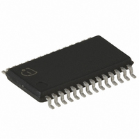
TDA5211 Infineon Technologies, TDA5211 Datasheet - Page 18

TDA5211
Manufacturer Part Number
TDA5211
Description
IC FSK/ASK RECEIVER P-TSSOP-28
Manufacturer
Infineon Technologies
Type
Receiverr
Datasheet
1.TDA5211.pdf
(52 pages)
Specifications of TDA5211
Package / Case
28-TSSOP
Frequency
310MHz ~ 350MHz
Sensitivity
-110dBm
Modulation Or Protocol
ASK, FSK
Applications
Alarm Systems, Communication Systems
Current - Receiving
5.7mA
Data Interface
PCB, Surface Mount
Antenna Connector
PCB, Surface Mount
Voltage - Supply
4.5 V ~ 5.5 V
Operating Temperature
-40°C ~ 105°C
Operating Frequency
350 MHz
Operating Supply Voltage
5 V
Maximum Operating Temperature
+ 150 C
Minimum Operating Temperature
- 40 C
Mounting Style
SMD/SMT
Operating Temperature (min)
-40C
Operating Temperature Classification
Automotive
Product Depth (mm)
4.4mm
Product Length (mm)
9.7mm
Operating Supply Voltage (min)
4.5V
Operating Supply Voltage (typ)
5V
Operating Supply Voltage (max)
5.5V
Lead Free Status / RoHS Status
Lead free / RoHS Compliant
Features
-
Memory Size
-
Data Rate - Maximum
-
Lead Free Status / Rohs Status
Compliant
Other names
SP000016390
TDA5211INTR
TDA5211XT
TDA5211XTINTR
TDA5211XTINTR
TDA5211INTR
TDA5211XT
TDA5211XTINTR
TDA5211XTINTR
Available stocks
Company
Part Number
Manufacturer
Quantity
Price
Part Number:
TDA5211
Manufacturer:
INFINEON/英飞凌
Quantity:
20 000
Part Number:
TDA5211B3
Manufacturer:
INFINEON/英飞凌
Quantity:
20 000
Company:
Part Number:
TDA5211B4
Manufacturer:
SIEMENS
Quantity:
5 510
Part Number:
TDA5211B4
Manufacturer:
INFINEON/英飞凌
Quantity:
20 000
Wireless Components
3.4.2
3.4.3
3.4.4
mined by connecting a capacitor to the TAGC pin (Pin 4) and should be chosen
along with the appropriate threshold voltage according to the intended operat-
ing case and interference scenario to be expected during operation. The opti-
mum choice of AGC time constant and the threshold voltage is described in
Section 4.1.
Mixer
The Double Balanced Mixer downconverts the input frequency (RF) in the
range of 310-350MHz to the intermediate frequency (IF) at 10.7MHz with a vol-
tage gain of approximately 21dB by utilising either high- or low-side injection of
the local oscillator signal. In case the mixer is interfaced only single-ended, the
unused mixer input has to be tied to ground via a capacitor. The mixer is fol-
lowed by a low pass filter with a corner frequency of 20MHz in order to suppress
RF signals to appear at the IF output (IFO pin). The IF output is internally con-
sisting of an emitter follower that has a source impedance of approximately
330 to facilitate interfacing the pin directly to a standard 10.7MHz ceramic filter
without additional matching circuitry.
PLL Synthesizer
The Phase Locked Loop synthesizer consists of a VCO, an asynchronous
divider chain, a phase detector with charge pump and a loop filter and is fully
implemented on-chip. The VCO is including spiral inductors and varactor
diodes. The FSEL pin (Pin11) has to be left open. The tuning range of the VCO
was designed to guarantee over production spread and the specified tempera-
ture range a receive frequency range between 310 and 350MHz depending on
whether high- or low-side injection of the local oscillator is used. The oscillator
signal is fed both to the synthesiser divider chain and to a divider that is dividing
the signal by 2 before it is applied to the downconverting mixer. Local oscillator
high side injection has to be used for receive frequencies between approxi-
mately 310 and 330 MHz, low side injection for receive frequencies between
330 and 350MHz - see also Section 4.4..
Crystal Oscillator
The on-chip crystal oscillator circuitry allows for utilisation of quartzes both in
the 5 and 10MHz range as the overall division ratio of the PLL can be switched
between 32 and 64 via the CSEL (Pin 16 ) pin according to the following table.
Table 3-2 CSEL Pin Operating States
CSEL
Open
Shorted to ground
3 - 10
Crystal Frequency
Functional Description
10.xx MHz
5.xx MHz
Specification, May 2001
TDA 5211


