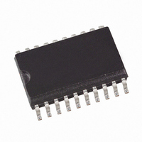
T5744N-TKQ Atmel, T5744N-TKQ Datasheet - Page 8

T5744N-TKQ
Manufacturer Part Number
T5744N-TKQ
Description
IC RCVR PLL ASK 450MHZ 20-SSOP
Manufacturer
Atmel
Datasheet
1.T5744N-TK.pdf
(19 pages)
Specifications of T5744N-TKQ
Frequency
300MHz ~ 450MHz
Sensitivity
-108dBm
Modulation Or Protocol
ASK
Applications
General Purpose Data Transmission Systems
Current - Receiving
30mA
Data Interface
PCB, Surface Mount
Antenna Connector
PCB, Surface Mount
Voltage - Supply
4.5 V ~ 5.5 V
Operating Temperature
-40°C ~ 105°C
Package / Case
20-SSOP
Lead Free Status / RoHS Status
Contains lead / RoHS non-compliant
Features
-
Memory Size
-
Data Rate - Maximum
-
Other names
T5744N-TKQTR
Receiving
Characteristics
Basic Clock Cycle of the
Digital Circuitry
8
T5744
The RF receiver T5744 can be operated with and without a SAW front-end filter. In a
typical automotive application, a SAW filter is used to achieve better selectivity. The
selectivity with and without a SAW front-end filter is illustrated in Figure 7. Note that the
mirror frequency is reduced by 40 dB. The plots are printed relatively to the maximum
sensitivity. If a SAW filter is used, an insertion loss of about 4 dB must be considered.
When designing the system in terms of receiving bandwidth, the LO deviation must be
considered as it also determines the IF center frequency. The total LO deviation is cal-
culated to be the sum of the deviation of the crystal and the XTO deviation of the T5744.
Low-cost crystals are specified to be within ±100 ppm. The XTO deviation of the T5744
is an additional deviation due to the XTO circuit. This deviation is specified to be
±30 ppm. If a crystal of ±100 ppm is used, the total deviation is ±130 ppm in that case.
Note that the receiving bandwidth and the IF-filter bandwidth are equivalent.
Figure 8. Receiving Frequency Response
The complete timing of the digital circuitry and the analog filtering is derived from one
clock. According to Figure 9, this clock cycle TClk is derived from the crystal oscillator
(XTO) in combination with a divider. The division factor is controlled by the logical state
at Pin MODE. According to chapter 'RF Front End', the frequency of the crystal oscillator
(f
of the local oscillator (f
Figure 9. Generation of the Basic Clock Cycle
XTO
) is defined by the RF input signal (f
-100.0
-20.0
-40.0
-60.0
-80.0
0.0
-6.0
LO
-5.0 -4.0
).
:14/:10
Divider
XTO
-3.0
T
f
Clk
XTO
-2.0
-1.0
RFin
df (MHz)
16
15
14
MODE
DVCC
XTO
0.0
) which also defines the operating frequency
1.0
without SAW
L : USA(:10)
H: Europe(:14)
2.0
with SAW
3.0
4.0
5.0
6.0
4521B–RKE–01/03


