CYRF69103-40LFXC Cypress Semiconductor Corp, CYRF69103-40LFXC Datasheet - Page 67
CYRF69103-40LFXC
Manufacturer Part Number
CYRF69103-40LFXC
Description
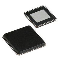
IC PROC 8K FLASH 40VQFN
Manufacturer
Cypress Semiconductor Corp
Series
CYRFr
Datasheet
1.CYRF69103-40LFXC.pdf
(68 pages)
Specifications of CYRF69103-40LFXC
Package / Case
40-VQFN Exposed Pad, 40-HVQFN, 40-SQFN, 40-DHVQFN
Frequency
2.4GHz
Data Rate - Maximum
1Mbps
Modulation Or Protocol
ISM
Applications
General Purpose
Power - Output
6dBm
Sensitivity
-87dBm
Voltage - Supply
1.8 V ~ 3.6 V
Current - Receiving
21.9mA
Current - Transmitting
39.9mA
Data Interface
PCB, Surface Mount
Memory Size
8kB Flash, 256B SRAM
Antenna Connector
PCB, Surface Mount
Operating Temperature
0°C ~ 70°C
Processor Series
CYRF691x
Core
M8C
Data Bus Width
8 bit
Data Ram Size
256 B
Interface Type
SPI
Maximum Clock Frequency
2 MHz
Number Of Programmable I/os
15
Number Of Timers
4
Operating Supply Voltage
2.5 V, 3.3 V
Maximum Operating Temperature
+ 70 C
Mounting Style
SMD/SMT
Minimum Operating Temperature
0 C
Program Memory Type
Flash
Program Memory Size
8 KB
Operating Temperature (min)
0C
Operating Temperature (max)
70C
Operating Temperature Classification
Commercial
Operating Supply Voltage (min)
1.8V
Operating Supply Voltage (typ)
2.5/3.3V
Operating Supply Voltage (max)
3.6V
Height
1 mm
Length
5.9 mm
Supply Voltage (max)
3.6 V
Supply Voltage (min)
1.8 V
Width
5.9 mm
Lead Free Status / RoHS Status
Lead free / RoHS Compliant
For Use With
770-1001 - ISP 4PORT CYPRESS ENCORE II MCU
Lead Free Status / Rohs Status
Lead free / RoHS Compliant
Other names
428-1933
Available stocks
Company
Part Number
Manufacturer
Quantity
Price

Part Number:
CYRF69103-40LFXC
Manufacturer:
CYCRESS
Quantity:
20 000


30. Document History Page
Document #: 001-07611 Rev *F
REV. ECN No.
Document Title: CYRF69103 Programmable Radio on Chip Low Power
Document #: 001-07611
*C
*D
*A
*B
*E
*F
**
2447906
2615458 KKU/AESA
2761532
2885149
479801
501282
631696
Change
Orig. of
AESA
DVJA
BOO
OYR
OYR
KKU
Submission
01/13/2009 Replaced 51-85190 with 001-12917. Fixed format and language inconsistencies.
09/09/2009 Changed default value of the Sleep Timer from 00(512 Hz) to 01(64 Hz) in the
02/26/2010 Updated the following sections:
See ECN
See ECN
See ECN
See ECN
Date
New advance data sheet.
Preliminary data sheet. Created Preliminary data sheet from Advance Information.
Final data sheet. Updated DC Characteristics table with characterization data.
Minor text changes
GPIO capacitance and timing diagram included
Sleep and Wakeup sequence documented
PIT Timer registers’ R/W capability corrected to read only
Updated radio function register descriptions
Changed L/D pin description
Changed RST Capacitor from 0.1 uF to 0.47 uF
Added example PMU configuration circuits
Updated to new template
OSC_CR0 [0x1E0] register.
Microcontroller
Mode,
troller Function Register
Sleep
Mode,
Function,
Low Power in Sleep
Summary, and
Clock Architecture
Description of Change
Mode,
Package Diagram
Description,
General Purpose I/O
CPU Clock During Sleep
CYRF69103
Ports,
Page 67 of 68
Microcon-
[+] Feedback
Related parts for CYRF69103-40LFXC
Image
Part Number
Description
Manufacturer
Datasheet
Request
R

Part Number:
Description:
IC PROC 8K FLASH 40-QFN
Manufacturer:
Cypress Semiconductor Corp
Part Number:
Description:
Manufacturer:
Cypress Semiconductor Corp
Datasheet:
Part Number:
Description:
Manufacturer:
Cypress Semiconductor Corp
Datasheet:
Part Number:
Description:
Manufacturer:
Cypress Semiconductor Corp
Datasheet:
Part Number:
Description:
Manufacturer:
Cypress Semiconductor Corp
Datasheet:
Part Number:
Description:
Manufacturer:
Cypress Semiconductor Corp
Datasheet: