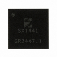
SX1441I077TRLF Semtech, SX1441I077TRLF Datasheet - Page 70

SX1441I077TRLF
Manufacturer Part Number
SX1441I077TRLF
Description
IC SYS-ON-CHIP BLUETOOTH 72LFBGA
Manufacturer
Semtech
Datasheet
1.SX1441EVK.pdf
(85 pages)
Specifications of SX1441I077TRLF
Frequency
2.4GHz
Modulation Or Protocol
Bluetooth v1.2, Class 2
Applications
Bluetooth v1.2
Voltage - Supply
2 V ~ 3.6 V
Current - Receiving
12.5mA
Data Interface
PCB, Surface Mount
Memory Size
4kByte ROM, 40kByte RAM
Antenna Connector
PCB, Surface Mount
Operating Temperature
-40°C ~ 85°C
Package / Case
72-LFBGA
Lead Free Status / RoHS Status
Lead free / RoHS Compliant
Power - Output
-
Sensitivity
-
Data Rate - Maximum
-
Current - Transmitting
-
Other names
SX1441I077LFTR
Personal Area Network
Equation 5 gives best estimation for the component values, since it does not take into account the resistance of the
inductor and assumes that the speaker impedance is resistive and constant over the whole frequency range.
However, the estimation is good starting point for the optimization of the components.
Choosing the filter cutoff frequency f
3.14.8 Volume Control
3.14.8.1
The data supplied to the DAC may be scaled digitally before analog conversion to provide volume amplification or
attenuation through the use of the RegVolCtrl and RegVolCmdDAC registers. The provided gain ranges from -
22.5dB (attenuation) to +22.5dB (amplification) in 1.5dB steps. Because such amplification is digital only, this
feature should be used only after optimum setting is chosen on the analog gain settings, so as not to increase
quantification noise level while maintaining proper SNR+THD levels.
Similarly, the data read from the ADC may be scaled before beeing transferred to the CPU in a similar manner.
Similarly to the DAC path, analog settings should be set at their optimum levels before using the digital volume
control.
3.14.8.2
Once volume control is enabled through setting the bit VolCtrEn in the RegVolCtrl register, the data from the ADC
(respectively DAC) path is digitally multiplied from a scaling factor derived from the ADCscaling bits from the
RegVolCmdADC register (respectively DACScaling from the RegVolCmdDAC register). The ADCscaling allows
the data to be amplified by up to 22.5dB or conversely attenuated by (up to) -22.5dB. The ADCscaling is applied
onto the data per formula :
Please note that although only 5 bits are relevant to the scaling, the ADCScaling value is an 8 bit signed integer.
3.15 DEBUG INTERFACE
3.15.1 Description
The debug interface can be used to observe and/or force the HCI UART and Codec signals. It can also be used as
a GPIO port.
3.15.2 Register Map
© Semtech 2006
Name
RegDbgDir
RegDbgOut
RegDbgIn
RegDbgMode
Pos
7-0
Pos
7-0
Description
ADC and DAC Scaling
RegDbgDir
DbgDir[7:0]
RegDbgOut
DbgOut[7:0]
ADCData
_
scaled
r/w
rw
r/w
rw
=
0
= 4 kHz and Z
sign
Table 129 – Debug interface registers
(
Table 131 - RegDbgOut register
Table 130 - RegDbgDir register
Reset
00000000
Reset
00000000
ADCScaling
L
= 32 Ω as typical values, gives L = 860 μH and C = 1 μF.
70
Function
DBG[7:0] pad direction
GPIO mode: 1 = output, 0 = input
Debug mode: 1 = observation, 0 = force
Function
DBG[7:0] pad output value. Valid only in GPIO mode
* )
Address (Hex)
0x0078
0x0079
0x007A
0x007B
max(
abs
(
ADCScaling
SX1441 – Bluetooth® 1.2 SoC
),
15
)
1 *
5 .
dB
www.semtech.com
*
ADCData
Data Sheet


