JN5148-001-M00T NXP Semiconductors, JN5148-001-M00T Datasheet - Page 8
JN5148-001-M00T
Manufacturer Part Number
JN5148-001-M00T
Description
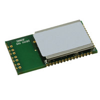
MODULE ZIGBEE PRO CERM ANTENNA
Manufacturer
NXP Semiconductors
Series
JN5148r
Specifications of JN5148-001-M00T
Frequency
2.4GHz
Modulation Or Protocol
802.15.4 Zigbee
Applications
AMR, ISM, Home Automation, Process Control
Power - Output
2.5dBm
Sensitivity
-95dBm
Voltage - Supply
2.3 V ~ 3.6 V
Current - Receiving
17.5mA
Current - Transmitting
15mA
Data Interface
PCB, Surface Mount
Memory Size
4Mbit Flash, 128kB RAM, 128kB ROM
Antenna Connector
On-Board, Chip
Operating Temperature
-40°C ~ 85°C
Package / Case
Module
Lead Free Status / RoHS Status
Lead free / RoHS Compliant
Data Rate - Maximum
-
Other names
616-1045-2
935294034534
JN5148-001-M00T
935294034534
JN5148-001-M00T


33
34
35
36
37
38
39
40
41
*: These two pins are not connected for High power modules
4.2. Pin Descriptions
All pins behave as described in the JN-DS-JN5148 Wireless Microcontroller Datasheet [2], with the exception of the
following:
4.2.1 Power Supplies
A single power supply pin, VDD is provided. Separate analogue (VSSA) and digital (GND) grounds are provided.
These should be connected together at the module pins.
4.2.2 SPI Memory Connections
SPISWP is a write protect pin for the serial flash memory. This should be held low to inhibit writes to the flash device.
SPISSZ is connected to SPI Slave Select 0 on the JN5148.
SPISSM is connected to the Slave Select pin on the memory.
This configuration allows the flash memory device to be programmed using an external SPI programmer if required.
For programming in this mode, the JN5148 should be held in reset by taking RESETN low. Two potential flash 4Mbit
memory devices may be used in the module, the Numonyx M25P40 and the SST SST25VF040B.
The memory can also be programmed over the UART by using the flash programmer software provided by Jennic.
This is available as part of the Software Developer kit and libraries available from www.nxp.com/jennic. To enter
this programming mode, SPIMISO (pin 7) should be held low whilst the chip is reset. Once programming has finished,
the chip should be reset, when it will execute the new code downloaded.
For normal operation of the module and programming over the UART, SPISSZ should be connected to
SPISSM.
8
COMP1+
COMP1-
DIO 20
DIO17
DIO18
DIO19
ADC1
ADC2
ADC3
CTS1
RTS1
TXD1
RXD1
IP_SEL
IP_INT
JN-DS-JN5148-001-Myy 1v4
DAI_SDOUT
DAI_SCK
JTAG_TMS
JTAG_TDO
JTAG_TCK
JTAG_TDI
CMOS
CMOS
CMOS
CMOS
3.3V
3.3V
3.3V
3.3V
3.3V
DIO17, UART 1 Clear To Send
Input, Intelligent Peripheral Device
Select Input or Digital Audio Clock
or JTAG CLK
DIO18, UART 1 Request To Send
Output, Intelligent Peripheral
Interrupt Output or Digital Audio
Data Output or JTAG Mode Select
DIO19 or UART 1 Transmit Data
Output or JTAG Data Out
DIO 20, UART 1 Receive Data
Input or JTAG data In
Comparator 1 Input -ve
Comparator 1 Input +ve
Analogue to Digital Input
Analogue to Digital Input
Analogue to Digital Input
© NXP Laboratories UK 2010
Related parts for JN5148-001-M00T
Image
Part Number
Description
Manufacturer
Datasheet
Request
R

Part Number:
Description:
Microcontrollers (MCU) 32bit RISC 32MHz
Manufacturer:
NXP Semiconductors
Datasheet:
Part Number:
Description:
Microcontrollers (MCU) 32bit RISC 32MHz
Manufacturer:
NXP Semiconductors

Part Number:
Description:
The JN5148 is an ultra low power, high performance MCU combined with an IEEE802
Manufacturer:
NXP Semiconductors
Datasheet:

Part Number:
Description:
Zigbee / 802.15.4 Modules & Development Tools Lo-Power RF Solution Jennic Demo Board
Manufacturer:
NXP Semiconductors
Datasheet:

Part Number:
Description:
Microcontrollers (MCU) 32bit RISC 2.4GHz
Manufacturer:
NXP Semiconductors
Datasheet:

Part Number:
Description:
KIT EVAL ZIGBEE PRO JN5148
Manufacturer:
Jennic LTD
Datasheet:

Part Number:
Description:
IC MCU 802.15.4 32BIT 2.4G 56QFN
Manufacturer:
NXP Semiconductors
Datasheet:

Part Number:
Description:
MODULE ZIGBEE PRO U.FL CONN
Manufacturer:
NXP Semiconductors
Datasheet:

Part Number:
Description:
MODULE ZIGBEE PRO HP U.FL CONN
Manufacturer:
NXP Semiconductors
Datasheet:

Part Number:
Description:
KIT UPGRADE ZIGBEE PRO
Manufacturer:
Jennic LTD
Datasheet:

Part Number:
Description:
MCU 802.15.4 32BIT 2.4G 56-QFN
Manufacturer:
NXP Semiconductors
Datasheet:
Part Number:
Description:
MCU 802.15.4 32BIT 2.4G 56-QFN
Manufacturer:
NXP Semiconductors
Datasheet:
Part Number:
Description:
Microcontrollers (MCU) 32bit RISC 32MHz
Manufacturer:
NXP Semiconductors

Part Number:
Description:
32BIT, MCU, ZIGBEE PRO, 128K RAM, 56QFN
Manufacturer:
Jennic LTD
Datasheet:

Part Number:
Description:
MODULE, ZIGBEE PRO, W/INTEGRATED ANT
Manufacturer:
Jennic LTD