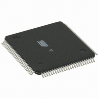
ATMEGA256RZBV-8AU Atmel, ATMEGA256RZBV-8AU Datasheet - Page 13

ATMEGA256RZBV-8AU
Manufacturer Part Number
ATMEGA256RZBV-8AU
Description
MCU ATMEGA2560/AT86RF230 100TQFP
Manufacturer
Atmel
Series
ATMEGAr
Datasheets
1.ATMEGA640V-8CU.pdf
(38 pages)
2.ATMEGA640V-8CU.pdf
(444 pages)
3.AT86RF230-ZU.pdf
(98 pages)
Specifications of ATMEGA256RZBV-8AU
Frequency
2.4GHz
Modulation Or Protocol
802.15.4 Zigbee
Applications
ISM, ZigBee™
Power - Output
3dBm
Sensitivity
-101dBm
Voltage - Supply
1.8 V ~ 3.6 V
Current - Receiving
15.5mA
Current - Transmitting
16.5mA
Data Interface
PCB, Surface Mount
Memory Size
256kB Flash, 4kB EEPROM, 8kB RAM
Antenna Connector
PCB, Surface Mount
Package / Case
100-TQFP
Wireless Frequency
2.4 GHz
Interface Type
JTAG, SPI
Output Power
3 dBm
Operating Temperature Range
- 55 C to + 125 C
For Use With
ATAVRISP2 - PROGRAMMER AVR IN SYSTEMATJTAGICE2 - AVR ON-CHIP D-BUG SYSTEM
Lead Free Status / RoHS Status
Lead free / RoHS Compliant
Operating Temperature
-
Data Rate - Maximum
-
Lead Free Status / Rohs Status
Lead free / RoHS Compliant
For Use With/related Products
ATmega256
Figure 6-6. Example SPI Sequence - Register Access Mode
6.2.2 Frame Buffer Access Modes
Figure 6-7. Packet Structure - Frame Buffer Write Access
SCLK
MOSI
MISO
5131E-MCU Wireless-02/09
SEL
Register Write Access
WRITE COMMAND
XX
Figure 6-5. Packet Structure – Register Read Access
Each register access must be terminated by setting SEL = H.
Figure 6-6 illustrates a typical SPI sequence for a register access sequence for write
and read respectively.
The Frame Buffer read access and the Frame Buffer write access are used to upload or
download frames to the microcontroller.
Each access starts by setting SEL = L. The first byte transferred on MOSI is the
command byte and must indicate a Frame Buffer access mode according to the
definition in Table 6-2.
On Frame Buffer write access the second byte transferred on MOSI contains the frame
length (PHR field) followed by the payload data (PSDU) as shown by Figure 6-7.
On Frame Buffer read access PHR and PSDU are transferred via MISO starting with
the second byte. After the PSDU data bytes one more byte can be transferred
containing the link quality indication (LQI) value of the received frame, for details refer
to section 8.5. Figure 6-8 illustrates the packet structure of a Frame Buffer read access.
Note, the Frame Buffer read access can be terminated at any time without any
consequences by setting SEL = H, e.g. after reading the frame length byte only.
MOSI
MISO
WRITE DATA
1
XX
byte 1 (command byte)
0
address[5:0]
XX
Register Read Access
read data[7:0]
byte 2 (data byte)
READ COMMAND
XX
XX
READ DATA
AT86RF230
XX
13


