AMIS-52150-XTD ON Semiconductor, AMIS-52150-XTD Datasheet - Page 9
AMIS-52150-XTD
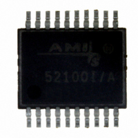
Manufacturer Part Number
AMIS-52150-XTD
Description
TXRX RF SUB 1GHZ CDR 20-SSOP
Manufacturer
ON Semiconductor
Datasheet
1.AMIS-52150-XTD.pdf
(25 pages)
Specifications of AMIS-52150-XTD
Frequency
300Mhz ~ 768MHz
Data Rate - Maximum
16kbps
Modulation Or Protocol
ASK, OOK
Applications
Wireless Modules
Power - Output
12dBm
Sensitivity
-117dBm
Voltage - Supply
2.3 V ~ 3.6 V
Current - Receiving
7.5mA
Current - Transmitting
25mA
Data Interface
PCB, Surface Mount
Antenna Connector
PCB, Surface Mount
Operating Temperature
0°C ~ 50°C
Package / Case
20-SSOP
Ic Interface Type
I2C
No. Of Tx Buffers
1
No. Of Rx Buffers
1
No. Of Filters
1
No. Of Interrupts
1
Supply Voltage Range
2.3V To 3.6V
Digital Ic Case Style
SSOP
No. Of Pins
20
Rohs Compliant
No
Operating Temperature (min)
0C
Operating Temperature Classification
Commercial
Modulation Type
ASK/OOK
Operating Supply Voltage (min)
2.3V
Operating Supply Voltage (typ)
3V
Operating Supply Voltage (max)
3.6V
Lead Free Status / RoHS Status
Lead free / RoHS Compliant
Memory Size
-
Lead Free Status / Rohs Status
Not Compliant
Other names
766-1020
Available stocks
Company
Part Number
Manufacturer
Quantity
Price
Company:

Part Number:
AMIS-52150-XTD
Manufacturer:
ON Semiconductor
Quantity:
135


AMIS-52150
8.6 GND, Ground Pin
The GND pin is the ground connection for the digital and analog circuits.
8.7 CLKOUT, Internal Clock Output Pin
The CLKOUT pin is an output for the RC oscillator, crystal oscillator signal or the recovered data clock, respectively. The crystal
oscillator signal output can be divided by 2, 3 or 4. The pin can also be programmed to output the signal from the recovered data clock
function. For more information about the clock and data recovery (CDR) function of the AMIS-52150, refer to the section of this
document on clock and data recovery.
The CLKOUT pin function control registers are shown in Table 13.
Table 13: Oscillator Output Control Registers
8.8 X1, X2, External Crystal Reference Pins
X1 and X2 pins connect a parallel resonance oscillator crystal to the AMIS-52150 internal oscillator circuit. The external crystal should
meet the requirements as listed in Table 14. However, the two load capacitors should be sized slightly smaller than the recommended
value for the crystal, because of the added capacitance due to the internal trim circuit. For further details, refer to the application note
titled “Quick Start Crystal Oscillator Circuit Operation and Set-up”. The crystal parameters are shown in Table 14.
Table 14: External Crystal Parameters
8.9 I
The AMIS-52150 implements an I
protocol for a slave device. The clock for the interface is generated by the external master device. The interface will support the normal
(0 – 100 Kbits/second) or the fast (0 – 400Kbits/second) data modes. The interface conforms to the Phillips specification for the I
standard. The pins have internal pull-up resistors. See Table 15 and Table 16 for some parameters of this interface.
In addition, Table 17 shows the details of register that controls the I
Table 15: Internal I
CLKOUT Pin Definition Control Registers
Register (HEX)
Parameter
Crystal frequency
Crystal ESR
Crystal tolerance
Load capacitance
2
CDATA, I
0x0c
0x0d
0x0e
2
CCLK, I
2
C Pull-up Resistors
Name
CLKOUT enable
CLKOUT select
XTAL divide
Load capacitors should be smaller than recommended for
the crystal to allow for frequency tuning
12.56
9.375
Min.
10.9
2
C Control Interface Bus Pins
Typ.
10
2
C serial 8-bit bi-directional interface with the pins I
12.65
Max.
24.0
14.0
70
Bits
4,5
0,1
7
Units
MHz
ppm
States
Ω
00
01
10
11
00
01
10
11
Rev. 7 | Page 9 of 25 | www.onsemi.com
0
1
Conditions
Targeted
Non-Quick Start
Quick Start
Comments
CLKOUT is enabled
CLKOUT is disabled
Automatic control
RC OSC
Xtal
Off
Divide by 4
Divide by 3
Divide by 2
Divide by 1
2
C address increment function.
2
CDATA and I
2
CCLK. The device implements the
2
C bus
Related parts for AMIS-52150-XTD
Image
Part Number
Description
Manufacturer
Datasheet
Request
R

Part Number:
Description:
ON Semiconductor [VOLTAGE REGULATOR]
Manufacturer:
ON Semiconductor
Datasheet:
Part Number:
Description:
357-036-542-201 CARDEDGE 36POS DL .156 BLK LOPRO
Manufacturer:
ON Semiconductor
Datasheet:
Part Number:
Description:
357-036-542-201 CARDEDGE 36POS DL .156 BLK LOPRO
Manufacturer:
ON Semiconductor
Datasheet:
Part Number:
Description:
357-036-542-201 CARDEDGE 36POS DL .156 BLK LOPRO
Manufacturer:
ON Semiconductor
Datasheet:
Part Number:
Description:
357-036-542-201 CARDEDGE 36POS DL .156 BLK LOPRO
Manufacturer:
ON Semiconductor
Datasheet:
Part Number:
Description:
357-036-542-201 CARDEDGE 36POS DL .156 BLK LOPRO
Manufacturer:
ON Semiconductor
Datasheet:
Part Number:
Description:
357-036-542-201 CARDEDGE 36POS DL .156 BLK LOPRO
Manufacturer:
ON Semiconductor
Datasheet:
Part Number:
Description:
357-036-542-201 CARDEDGE 36POS DL .156 BLK LOPRO
Manufacturer:
ON Semiconductor
Datasheet:
Part Number:
Description:
357-036-542-201 CARDEDGE 36POS DL .156 BLK LOPRO
Manufacturer:
ON Semiconductor
Datasheet:
Part Number:
Description:
357-036-542-201 CARDEDGE 36POS DL .156 BLK LOPRO
Manufacturer:
ON Semiconductor
Datasheet:
Part Number:
Description:
357-036-542-201 CARDEDGE 36POS DL .156 BLK LOPRO
Manufacturer:
ON Semiconductor
Datasheet:
Part Number:
Description:
Manufacturer:
ON Semiconductor
Datasheet:
Part Number:
Description:
Manufacturer:
ON Semiconductor
Datasheet:
Part Number:
Description:
Manufacturer:
ON Semiconductor
Datasheet: