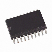
U7004B-MFSG3 Atmel, U7004B-MFSG3 Datasheet

U7004B-MFSG3
Specifications of U7004B-MFSG3
Available stocks
Related parts for U7004B-MFSG3
U7004B-MFSG3 Summary of contents
Page 1
... Electrostatic sensitive device. Observe precautions for handling. Description The U7004B is a monolithic SiGe transmit/receive front end IC with power amplifier, 50- W internal matching, low-noise amplifier and T/R switch driver especially designed for operation in TDMA systems like DECT. Due to the ramp-control feature and a very low quiescent current, an external switch transistor for V Figure 1 ...
Page 2
... Power amplifier input 16 VS_LNA Supply-voltage input for low-noise amplifier 17 GND8 Ground 18 LNA_OUT Low-noise amplifier output 19 RX_ON RX active high 20 PU Power-up active high U7004B 2 1 R_SWITCH 2 SWITCH_OUT GND1 3 LNA_IN 4 U7004B 5 GND2 V1_PA 6 7 GND3 8 GND4 9 GND5 10 V2_PA_OUT RX_ON 18 LNA_OUT 17 GND8 16 VS_LNA 15 PA_IN 14 ...
Page 3
... Typ. Max. 3.6 4.6 3.6 4.6 450 8 10 +25 +70 = 417 µs on Symbol Min. Typ. Max. V 2.7 3.6 4 450 S_TX I 10 S_RX I 10 S_standby f 1.88 1. DGp 48 U7004B Unit °C °C dBm dBm Unit K/W Unit µA °C Unit V mA µA µA GHz ...
Page 4
... Notes: 1. Power amplifier shall be unconditionally stable, maximum duty cycle 50%, maximum load mismatch and duration: load VSWR = 20:1 (all phases With external matching network (see Figure 13 and Figure 14) 3. Low-noise amplifier shall be unconditionally stable U7004B 25°C, pulsed mode, duty cycle 4.17 ...
Page 5
... Table 1. Control Logic for LNA and T/R Switch Driver Operation Mode Standby TX RX Figure 3. Output Power versus Ramp Voltage Input/Output Circuits Figure 4. Input Circuit PA_IN/VS_PA 4713A–DECT–07/ -10 -20 0.0 0.5 1.0 1.5 V (V) RAMP 13 VS_PA 15 PA_IN 17 GND1 U7004B RX_ON 2.0 2.5 3.0 5 ...
Page 6
... Figure 5. Input Circuit RAMP/VS_PA Figure 6. Input Circuit V1_PA Figure 7. Input/Output Circuit V2_PA U7004B 6 13 VS_PA 14 RAMP 7 GND7 6 V1_PA 8 GND3 10 V2_PA_OUT 8 GND5 4713A–DECT–07/03 ...
Page 7
... Figure 8. Input Circuit LNA_IN/VS_LNA Figure 9. Output Circuit LNA_OUT 4713A–DECT–07/03 16 VS_LNA 4 LNA_IN 3 GND1 16 VS_LNA 18 LNA_OUT 5 GND2 U7004B 7 ...
Page 8
... Figure 10. Input Circuit SWITCH_OUT/R_SWITCH Figure 11. Input Circuit RX_ON Figure 12. Input Circuit PU U7004B 8 13 VS_PA 2 SWITCH_OUT R_SWITCH 17 GND8 16 VS_LNA 19 RX_ON 16 VS_LNA 4713A–DECT–07/03 ...
Page 9
... Typical Application Circuit Figure 13. Typical Schematic PU RX_ON 20 TX/RX standby control 1 4713A–DECT–07/03 LNA_OUT PA_IN RAMP U7004B TX LNA PCB diel. BPF Microstripline l/4 PCB PCB VS PCB Antenna U7004B 9 ...
Page 10
... Figure 14. U7004B Application Board Schematic Figure 15. U7004B Application Board Layout U7004B 10 LNA_OUT DECT Frontend 0R 100 pF 56pF V1_PA 0R VS_PA 0R 2.7 k 390 0R LNA_IN PA_IN RAMP 2 22nH 4.7 mF 1.2 pF 1.0 pF 15nH 0R 56pF 1nF 0R 1mF Components Inductors (Pins 10,13,15) 0R V2_PA - 16 Capacitors - 1 Resistor (Pin 1) ...
Page 11
... Ordering Information Extended Type Number U7004B-MFS U7004B-MFSG3 Package Information Package SSO20 Dimensions in mm 0.25 0. 4713A–DECT–07/03 Package Remarks SSO20 Tube SSO20 Taped and reeled 6.75 6.50 1.30 0.15 0.05 5.85 11 technical drawings according to DIN specifications 10 U7004B 5.7 5.3 4.5 4.3 ...
Page 12
... No licenses to patents or other intellectual property of Atmel are granted by the Company in connection with the sale of Atmel products, expressly or by implication. Atmel’s products are not authorized for use as critical components in life support devices or systems. ...


