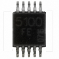
TDK5100F Infineon Technologies, TDK5100F Datasheet - Page 29

TDK5100F
Manufacturer Part Number
TDK5100F
Description
TRANSMITTER ASK/FSK SGL TSSOP10
Manufacturer
Infineon Technologies
Type
Transmitterr
Datasheet
1.TDK5100F.pdf
(39 pages)
Specifications of TDK5100F
Package / Case
10-TSSOP
Frequency
434MHz Center
Applications
Alarm Systems, Communication Systems
Modulation Or Protocol
ASK, FSK
Data Rate - Maximum
20 kbps
Power - Output
3.2dBm
Current - Transmitting
7mA
Data Interface
PCB, Surface Mount
Antenna Connector
PCB, Surface Mount
Voltage - Supply
2.1 V ~ 4 V
Operating Temperature
-25°C ~ 85°C
Operating Frequency
435 MHz
Operating Supply Voltage
2.5 V, 3.3 V
Maximum Operating Temperature
+ 125 C
Minimum Operating Temperature
- 40 C
Mounting Style
SMD/SMT
Operating Temperature (min)
-40C
Operating Temperature (max)
125C
Operating Temperature Classification
Automotive
Operating Supply Voltage (min)
2.1V
Operating Supply Voltage (typ)
2.5/3.3V
Lead Free Status / RoHS Status
Lead free / RoHS Compliant
Features
-
Memory Size
-
Lead Free Status / Rohs Status
Compliant
Other names
SP000014745
TDK5100F
TDK5100FINTR
TDK5100FXT
TDK5100F
TDK5100FINTR
TDK5100FXT
Available stocks
Company
Part Number
Manufacturer
Quantity
Price
Company:
Part Number:
TDK5100F
Manufacturer:
ST
Quantity:
2 100
Company:
Part Number:
TDK5100F
Manufacturer:
Infineon Technologies
Quantity:
135
Part Number:
TDK5100F
Manufacturer:
INFINEON/英飞凌
Quantity:
20 000
Part Number:
TDK5100FHTMA1
Manufacturer:
INFINEON/英飞凌
Quantity:
20 000
In practice the RF-saturation voltage of the PA transistor and other parasitics reduce the
“critical” R
The output power P
R
The power efficiency (and the bandwidth) increase when operating at a slightly higher
R
The collector efficiency E is defined as
The diagram of Figure 17 was measured directly at the PA-output at V
the matching circuitry decrease the output power by about 1.5 dB. As can be seen from
the diagram, 550 Ω is the optimum impedance for operation at 3 V. For an approximation
of R
and
Figure 17
The DC collector current I
the load resistor R
collector current will show a characteristic dip at the resonance frequency for this type of
“overcritical” operation. The depth of this dip will increase with higher values of R
Data Sheet
L
L
, as shown in Figure 17.
> R
OPT
LC
and P
.
LC
.
OUT
Output power P
10*E
Po [mW]
at other supply voltages those two formulas can be used:
L
. This is typical for overcritical operation of class C amplifiers. The
o
7
6
5
4
3
2
1
0
is reduced by operating in an “overcritical” mode characterised by
0
c
of the power amplifier and the RF output power P
o
(mW) and collector efficiency E vs. load resistor R
1000
P
E =
R
OUT
OPT
29
V
2000
~
P
~
S
O
I
R
V
C
OPT
S
RL [Ohm]
3000
10*E
Po
S
V 1.2, 2008-04-04
= 3 V. Losses in
Applications
TDK5100F
o
vary with
L
L
.
.


