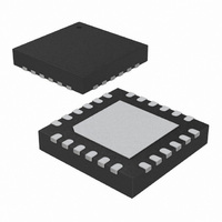
ATA8742-PXQW Atmel, ATA8742-PXQW Datasheet - Page 119

ATA8742-PXQW
Manufacturer Part Number
ATA8742-PXQW
Description
MCU W/TRANSMITTER ASK/FSK 24QFN
Manufacturer
Atmel
Datasheet
1.ATA8742-PXQW.pdf
(238 pages)
Specifications of ATA8742-PXQW
Frequency
433MHz
Applications
Home Automation, Remote Sensing, RKE
Modulation Or Protocol
ASK, FSK
Data Rate - Maximum
32 kBit/s
Power - Output
7.5dBm
Current - Transmitting
9.8mA
Data Interface
PCB, Surface Mount
Antenna Connector
PCB, Surface Mount
Memory Size
4kB Flash, 256B EEPROM, 256B SRAM
Voltage - Supply
2 V ~ 4 V
Operating Temperature
-40°C ~ 85°C
Package / Case
24-VQFN Exposed Pad, 24-HVQFN, 24-SQFN, 24-DHVQFN
Processor Series
ATA8x
Core
AVR8
Data Bus Width
8 bit
Program Memory Type
Flash
Program Memory Size
4 KB
Data Ram Size
256 B
Interface Type
SPI, USI
Maximum Clock Frequency
8.1 MHz
Number Of Programmable I/os
12
Number Of Timers
2
Maximum Operating Temperature
+ 85 C
Mounting Style
SMD/SMT
Development Tools By Supplier
ATASTK512-EK1-IND
Minimum Operating Temperature
- 40 C
On-chip Adc
10 bit, 8 Channel
Lead Free Status / RoHS Status
Lead free / RoHS Compliant
Features
-
Lead Free Status / Rohs Status
Details
Available stocks
Company
Part Number
Manufacturer
Quantity
Price
Company:
Part Number:
ATA8742-PXQW
Manufacturer:
ATMEL
Quantity:
1 482
- Current page: 119 of 238
- Download datasheet (4Mb)
21.8.1
21.9
21.9.1
21.9.2
9151A–INDCO–07/09
Modes of Operation
Compare Output Mode and Waveform Generation
Normal Mode
Clear Timer on Compare Match (CTC) Mode
The Waveform Generator uses the COM1x1:0 bits differently in normal, CTC, and PWM modes.
For all modes, setting the COM1x1:0 = 0 tells the Waveform Generator that no action on the
OC1x Register is to be performed on the next compare match. For compare output actions in the
non-PWM modes refer to
page
page
A change of the COM1x1:0 bits state will have effect at the first compare match after the bits are
written. For non-PWM modes, the action can be forced to have immediate effect by using the 1x
strobe bits.
The mode of operation, i.e., the behavior of the Timer/Counter and the Output Compare pins, is
defined by the combination of the Waveform Generation mode (WGM13:0) and Compare Output
mode (COM1x1:0) bits. The Compare Output mode bits do not affect the counting sequence,
while the Waveform Generation mode bits do. The COM1x1:0 bits control whether the PWM out-
put generated should be inverted or not (inverted or non-inverted PWM). For non-PWM modes
the COM1x1:0 bits control whether the output should be set, cleared or toggle at a compare
match
For detailed timing information refer to
The simplest mode of operation is the Normal mode (WGM13:0 = 0). In this mode the counting
direction is always up (incrementing), and no counter clear is performed. The counter simply
overruns when it passes its maximum 16-bit value (MAX = 0xFFFF) and then restarts from the
BOTTOM (0x0000). In normal operation the Timer/Counter Overflow Flag (TOV1) will be set in
the same timer clock cycle as the TCNT1 becomes zero. The TOV1 flag in this case behaves
like a 17th bit, except that it is only set, not cleared. However, combined with the timer overflow
interrupt that automatically clears the TOV1 flag, the timer resolution can be increased by soft-
ware. There are no special cases to consider in the Normal mode, a new counter value can be
written anytime.
The Input Capture unit is easy to use in Normal mode. However, observe that the maximum
interval between the external events must not exceed the resolution of the counter. If the interval
between events are too long, the timer overflow interrupt or the prescaler must be used to
extend the resolution for the capture unit.
The Output Compare units can be used to generate interrupts at some given time. Using the
Output Compare to generate waveforms in Normal mode is not recommended, since this will
occupy too much of the CPU time.
In Clear Timer on Compare or CTC mode (WGM13:0 = 4 or 12), the OCR1A or ICR1 Register
are used to manipulate the counter resolution. In CTC mode the counter is cleared to zero when
the counter value (TCNT1) matches either the OCR1A (WGM13:0 = 4) or the ICR1 (WGM13:0 =
12). The OCR1A or ICR1 define the top value for the counter, hence also its resolution. This
mode allows greater control of the compare match output frequency. It also simplifies the opera-
tion of counting external events.
129, and for phase correct and phase and frequency correct PWM refer to
130.
(“Compare Match Output Unit” on page
Table 21-1 on page
“Timer/Counter Timing Diagrams” on page
118)
129. For fast PWM mode refer to
ATA8742
Table 21-2 on
Table 21-3 on
126.
119
Related parts for ATA8742-PXQW
Image
Part Number
Description
Manufacturer
Datasheet
Request
R

Part Number:
Description:
Manufacturer:
ATMEL Corporation
Datasheet:

Part Number:
Description:
DEV KIT FOR AVR/AVR32
Manufacturer:
Atmel
Datasheet:

Part Number:
Description:
INTERVAL AND WIPE/WASH WIPER CONTROL IC WITH DELAY
Manufacturer:
ATMEL Corporation
Datasheet:

Part Number:
Description:
Low-Voltage Voice-Switched IC for Hands-Free Operation
Manufacturer:
ATMEL Corporation
Datasheet:

Part Number:
Description:
MONOLITHIC INTEGRATED FEATUREPHONE CIRCUIT
Manufacturer:
ATMEL Corporation
Datasheet:

Part Number:
Description:
AM-FM Receiver IC U4255BM-M
Manufacturer:
ATMEL Corporation
Datasheet:

Part Number:
Description:
Monolithic Integrated Feature Phone Circuit
Manufacturer:
ATMEL Corporation
Datasheet:

Part Number:
Description:
Multistandard Video-IF and Quasi Parallel Sound Processing
Manufacturer:
ATMEL Corporation
Datasheet:

Part Number:
Description:
High-performance EE PLD
Manufacturer:
ATMEL Corporation
Datasheet:

Part Number:
Description:
8-bit Flash Microcontroller
Manufacturer:
ATMEL Corporation
Datasheet:

Part Number:
Description:
2-Wire Serial EEPROM
Manufacturer:
ATMEL Corporation
Datasheet:


