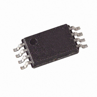
T48C862M-R4-TNS Atmel, T48C862M-R4-TNS Datasheet - Page 74

T48C862M-R4-TNS
Manufacturer Part Number
T48C862M-R4-TNS
Description
IC MON TIRE PRESS 433MHZ 24-SOIC
Manufacturer
Atmel
Datasheet
1.T48C862M-R4-TNS.pdf
(107 pages)
Specifications of T48C862M-R4-TNS
Frequency
433MHz
Modulation Or Protocol
FM, FSK
Data Rate - Maximum
32 kBaud
Power - Output
10dBm
Current - Transmitting
9.5mA
Data Interface
PCB, Surface Mount
Antenna Connector
PCB, Surface Mount
Memory Size
1KB EEPROM, 1KB RAM
Voltage - Supply
2 V ~ 4 V
Operating Temperature
-40°C ~ 125°C
Package / Case
24-SOIC (0.200", 5.30mm Width)
Lead Free Status / RoHS Status
Contains lead / RoHS non-compliant
Features
-
Applications
-
SSI Interrupt
Modulation and Demodulation
74
T48C862-R4 [Preliminary]
The SSI interrupt INT3 can be generated either by an SSI buffer register status (i.e.,
transmit buffer empty or receive buffer full), the end of SSI data telegram or on the fall-
ing edge of the SC/SD pins on Port 4 (see “Port 4 Control Register (P4CR) Byte Write”
on page 38). SSI interrupt selection is performed by the Interrupt FunctioN control bit
(IFN). The SSI interrupt is usually used to synchronize the software control of the SSI
and inform the controller of the present SSI status. The Port 4 interrupts can be used
together with the SSI or, if the SSI itself is not required, as additional external interrupt
sources. In either case this interrupt is capable of waking the controller out of sleep
mode.
To enable and select the SSI relevant interrupts use the SSI interrupt mask (SIM) and
the Interrupt Function (IFN) while the Port 4 interrupts are enabled by setting appropri-
ate control bits in P4CR register.
If the shift register is used together with Timer 2 or Timer 3 for modulation or demodula-
tion purposes, the 8-bit synchronous mode must be used. In this case, the unused Port
4 pins can be used as conventional bi-directional ports.
The modulation and demodulation stages, if enabled, operate as soon as the SSI is acti-
vated (SIR = 0) and cease when deactivated (SIR = 1).
Due to the byte-orientated data control, the SSI (when running normally) generates
serial bit streams which are submultiples of 8 bits. An SSI output masking (OMSK) func-
tion permits; however, the generation of bit streams of any length. The OMSK signal is
derived indirectly from the 4-bit prescaler of the Timer 2 and masks out a programmable
number of unrequired trailing data bits during the shifting out of the final data word in the
bit stream. The number of non-masked data bits is defined by the value pre-pro-
grammed in the prescaler compare register. To use output masking, the modulator stop
mode bit (MSM) must be set to "0" before programming the final data word into the SSI
transmit buffer. This in turn, enables shift clocks to the prescaler when this final word is
shifted out. On reaching the compare value, the prescaler triggers the OMSK signal and
all following data bits are blanked.
Figure 72. SSI Output Masking Function
T1OUT
SYSCL
TOG2
POUT
SCL
/2
SC
CL2/1
Shift_CL
4-bit counter 2/1
Compare 2/1
SO
CM1
MSB
SSI-control
8-bit shift register
LSB
Control
Timer 2
OMSK
4551C–4BMCU–01/04
SI
Output
SO


