SCP1000-D11 VTI Technologies, SCP1000-D11 Datasheet - Page 25
SCP1000-D11
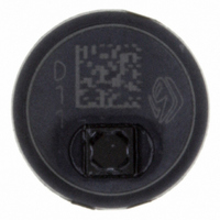
Manufacturer Part Number
SCP1000-D11
Description
SENSOR I2C 30-120KPA
Manufacturer
VTI Technologies
Series
SCP1000r
Datasheet
1.SCP1000_PCB3.pdf
(37 pages)
Specifications of SCP1000-D11
Pressure Type
Absolute
Operating Pressure
4.35 ~ 17.40 PSI, 30 ~ 120 kPa
Output
Digital
Voltage - Supply
2.4 V ~ 3.3 V
Termination Style
Surface Mount
Operating Temperature
-20°C ~ 70°C
Package / Case
PCB Mount
Lead Free Status / RoHS Status
Lead free / RoHS Compliant
Other names
551-1043-2
Available stocks
Company
Part Number
Manufacturer
Quantity
Price
Company:

Part Number:
SCP1000-D11
Manufacturer:
ST
Quantity:
1 001
Part Number:
SCP1000-D11
Manufacturer:
VTI
Quantity:
20 000


4.2 TWI Interface
4.2.1
VTI Technologies Oy
www.vti.fi
TWI frame format
TWI is a 2-wire half-duplex serial interface. It consists of one master device and one or more slave
devices. The master is defined as a micro controller providing the serial clock (SCL), and the slave
as any integrated circuit receiving the SCL clock from the master. The SCP1000 sensor always
operates as a slave device in master-slave operation mode. When in SPI interface a hardware
addressing is used (slaves have dedicated CSB signals), the TWI interface uses a software based
addressing (slave devices have dedicated bit patterns as addresses). Seven bit device addressing
is used with SCP1000. The default TWI device address for SCP1000 is 0x11, b’001 0001’ (pre-
programmed during SCP1000 production).
The two wires in TWI bus are:
The SCL pin of SCP1000 is an input pin (SCP1000 never controls the SCL line). Data is
transferred in and out of the sensor through the bi-directional SDA pin. SDA has an open-drain
output, so an external pull-up resistor to DVDD is required (see Figure 11). The minimum value for
SDA pull-up resistor is 2 kΩ.
External pull-up resistor from SCL to DVDD is not needed if master drives SCL actively to high and
low states. There is no de-bouncing is implemented in the SCP1000 digital I/O pads, so the signals
on SDA and SCL must be clean.
TWI transactions are based on a byte-long transfers separated by acknowledgements. Bits from
SDA line are sampled in on the rising edge of SCL and bits to SDA line are latched out on falling
edge of SCL. Master starts and stops the communication by sending start and stop bits. After start
bit master sends device TWI device address. The communication continues with predefined frame
format. General patterns of TWI frame format are described below.
Figure 11. TWI master slave configuration.
µC (Master)
o
o
SCL, serial clock and
SDA, bi-directional data line.
START BIT (µC → SCP1000)
The start bit is a high to low transition on SDA, while SCL is high. When the master
issues a start bit, it takes the control of the bus.
SLAVE DEVICE ADDRESS (µC → SCP1000)
Master sends a 7 bit slave device address, bits [7:1], MSB first. SCP1000 device
address is 0x11, b’001 0001’ by default. The LSB (bit 0) indicates the type of access
(‘1’ = Read or ‘0’ = Write).
ACKNOWLEDGE BIT
The transmitter of the acknowledge bit must tie the SDA line to low to perform an
acknowledgement. The receiver of the acknowledge bit must release the SDA line
because at this time, it is not the master of the TWI bus. The receiver then checks
the acknowledge bit by reading a ‘0’ on SDA.
External pull-up resistor to DVDD
Doc.Nr. 8260800.08
SDA
SCL
Subject to changes
SCP1000 (Slave)
TWI
SCP1000 Series
Rev.0.08
25/37
Related parts for SCP1000-D11
Image
Part Number
Description
Manufacturer
Datasheet
Request
R


Part Number:
Description:
SENSOR 30-120KPA SPI
Manufacturer:
VTI Technologies
Datasheet:

Part Number:
Description:
SENSOR I2C 30-120KPA PCB
Manufacturer:
VTI Technologies
Datasheet:

Part Number:
Description:
SENSOR SPI 30-120KPA PCB
Manufacturer:
VTI Technologies
Datasheet:

Part Number:
Description:
Manufacturer:
Samtec Inc
Datasheet:
Part Number:
Description:
SEALED CIRCULAR POWER CABLE PLUG
Manufacturer:
Samtec Inc

Part Number:
Description:
ACCELEROMETER SGL 1.7G DIL8 SMD
Manufacturer:
VTI Technologies
Datasheet:

Part Number:
Description:
VTI Automotive Digital Accelerometer Platform
Manufacturer:
VTI [VTI technologies]
Datasheet:

Part Number:
Description:
BOARD PWB ACCEL 3-AXIS SPI/I2C
Manufacturer:
VTI Technologies
Datasheet:

Part Number:
Description:
EVAL BOARD ACCELEROMETER Y-AXIS
Manufacturer:
VTI Technologies
Datasheet:
Part Number:
Description:
ACCELEROMETER SGL 1.7G DIL8 SMD
Manufacturer:
VTI Technologies
Datasheet:
Part Number:
Description:
VTI Automotive Digital Accelerometer Platform
Manufacturer:
VTI [VTI technologies]
Datasheet:
Part Number:
Description:
Accelerometer
Manufacturer:
VTI [VTI technologies]
Datasheet:
Part Number:
Description:
Stand Alone Inclinometer
Manufacturer:
VTI [VTI technologies]
Datasheet:
Part Number:
Description:
3-axis accelerometer
Manufacturer:
VTI [VTI technologies]
Datasheet: