TBU-CA065-100-WH Bourns Inc., TBU-CA065-100-WH Datasheet - Page 3
TBU-CA065-100-WH
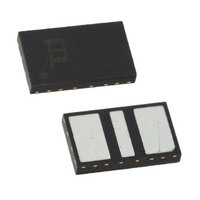
Manufacturer Part Number
TBU-CA065-100-WH
Description
SURGE SUPP TBU 100MA 650VIMP SMD
Manufacturer
Bourns Inc.
Series
TBU-CAr
Datasheet
1.TBU-CA040-050-WH.pdf
(6 pages)
Specifications of TBU-CA065-100-WH
Package / Case
SMD 6.50mm x 4.00mm
Voltage - Working
300V
Voltage - Clamping
650V
Technology
Mixed Technology
Number Of Circuits
2
Applications
General Purpose
Voltage Rating
650 V
Current Rating
100 mA
Operating Temperature Range
- 40 C to + 125 C
Termination Style
SMD/SMT
Lead Free Status / RoHS Status
Lead free / RoHS Compliant
Power (watts)
-
Lead Free Status / Rohs Status
Lead free / RoHS Compliant
Other names
TBU-CA065-100-WHTR
Available stocks
Company
Part Number
Manufacturer
Quantity
Price
Company:

Part Number:
TBU-CA065-100-WH
Manufacturer:
BOURNS
Quantity:
1 372
Part Number:
TBU-CA065-100-WH
Manufacturer:
BOURNS/伯恩斯
Quantity:
20 000


The TBU
variety of applications. The maximum voltage rating of the TBU
device should never be exceeded. Where necessary, an OVP
should be employed to limit the maximum voltage. A cost-
effective protection solution combines Bourns
devices with a pair of Bourns
applications, a Bourns
Specifi cations are subject to change without notice.
Customers should verify actual device performance in their specifi c applications.
Reference Application
Performance Graphs
Typical V-I Characteristics (TBU-CA050-300-WH)
Power Derating Curve
TBU-CA Series - TBU
Equip.
®
devices are general use protectors used in a wide
3.0
2.5
2.0
1.5
1.0
0.5
0.0
20
40
Line Out
/ Line In
Line Out
/ Line In
®
TBU
Device
Device
TBU
CURRENT
(100 mA/div)
GDT may be substituted for the MOV.
Ambient Temperature (°C)
60
TM
TM
®
MOVs. For bandwidth sensitive
80
No Additional PCB Cu
0.5 sq. in. Additional PCB Cu
100
®
I
TRIP
High-Speed Protectors
VOLTAGE
(5 V/div)
V
120
RESET
Line In /
Line Out
Line In /
Line Out
®
TBU
140
OVP
OVP
®
protection
Line
Line
®
The TBU
technology, placed in the system circuit will monitor the
current with the MOSFET detection circuit triggering to provide
an effective barrier behind which sensitive electronics are not
exposed to large voltages or currents during surge events. The
TBU
current exceeds the TBU
When operated, the TBU
than 1 mA typically. When operated, the TBU
block all voltages including the surge up to rated limits.
After the surge, the TBU
across the TBU
device will automatically reset on lines which have no DC bias
or have DC bias below V
If the line has a normal DC bias above V
across the TBU
surge. In such cases, special care needs to be taken to ensure
that the TBU
one method used to accomplish this. Bourns application
engineers can provide further assistance.
Typical Trip Current vs. Temperature
Typical Resistance vs. Temperature
Basic TBU Operation
®
device operates in approximately 1 µs - once line
®
device, constructed using MOSFET semiconductor
®
1.8
1.6
1.4
1.2
1.0
0.8
0.6
0.4
0.2
0.0
device will reset, with software monitoring as
2.2
2.0
1.8
1.6
1.4
1.2
1.0
0.8
0.6
0.4
0.2
0.0
®
®
-75 -50 -25
-75 -50 -25
device falls to the V
device may not fall below V
Junction Temperature (°C)
Junction Temperature (°C)
®
reset
®
®
device resets when the voltage
device restricts line current to less
device’s trigger current Itrigger.
0
0
(such as unpowered signal lines).
25
25
50
50
reset
75 100 125 150
75 100 125 150
reset
level. The TBU
, the voltage
reset
®
device will
after the
®
Related parts for TBU-CA065-100-WH
Image
Part Number
Description
Manufacturer
Datasheet
Request
R

Part Number:
Description:
SURGE SUPP TBU 200MA 650VIMP SMD
Manufacturer:
Bourns Inc.
Datasheet:
Part Number:
Description:
SURGE SUPP TBU 300MA 650VIMP SMD
Manufacturer:
Bourns Inc.
Datasheet:
Part Number:
Description:
SURGE SUPP TBU 50MA 650VIMP SMD
Manufacturer:
Bourns Inc.
Datasheet:
Part Number:
Description:
SURGE SUPP TBU 500MA 650VIMP SMD
Manufacturer:
Bourns Inc.
Datasheet:

Part Number:
Description:
TBU EVAL BOARD PORT RS-485
Manufacturer:
Bourns Inc.
Datasheet:

Part Number:
Description:
Manufacturer:
Bourns, Inc.
Datasheet:
Part Number:
Description:
11mm Potentiometer
Manufacturer:
Bourns, Inc.
Datasheet:
Part Number:
Description:
Manufacturer:
Bourns, Inc.
Datasheet:
Part Number:
Description:
Manufacturer:
Bourns, Inc.
Datasheet:
Part Number:
Description:
Manufacturer:
Bourns, Inc.
Datasheet:
Part Number:
Description:
5/16 Round Trimming Potentiometer
Manufacturer:
Bourns, Inc.
Datasheet: