CDDFN2-T12C Bourns Inc., CDDFN2-T12C Datasheet

TVS DIODE 12V 25W BI SMD

CDDFN2-T12C

Manufacturer Part Number
CDDFN2-T12C
Description
TVS DIODE 12V 25W BI SMD
Manufacturer
Bourns Inc.
Series
CDr
Datasheet

Specifications of CDDFN2-T12C

Package / Case
2-UFDFN
Voltage - Reverse Standoff (typ)
12V
Voltage - Breakdown
13V
Power (watts)
25W
Polarization
Bidirectional
Mounting Type
Surface Mount
Polarity
Bidirectional
Channels
1 Channel
Clamping Voltage
25 V
Operating Voltage
12 V
Breakdown Voltage
13 V
Termination Style
SMD/SMT
Peak Surge Current
1 A
Capacitance
12 pF
Maximum Operating Temperature
+ 125 C
Minimum Operating Temperature
- 40 C
Dimensions
0.55 mm W x 0.95 mm L x 0.45 mm H
Mounting Style
SMD/SMT
Reverse Stand-off Voltage Vrwm
12V
Clamping Voltage Vc Max
25V
Diode Configuration
Bidirectional
Peak Pulse Current Ippm
1A
Diode Case Style
DFN
No. Of Pins
2
Diode Type
Bidirectional TVS
Breakdown Voltage Vbr
13V
Lead Free Status / RoHS Status
Lead free / RoHS Compliant
Lead Free Status / RoHS Status
Lead free / RoHS Compliant, Lead free / RoHS Compliant
Other names
CDDFN2-T12CTR
The CDDFN2-TxxC Series provides ESD and EFT protection for external ports of electronic devices
such as cellular phones, hand held electronics and other portable electronic devices.
The device measures 1.05 mm x 0.65 mm and is available in a DFN-2 package and is intended to be
mounted directly onto an FR4 printed circuit board. The device will fi t an 0402 footprint.
The device is designed to meet IEC 61000-4-2(ESD) and IEC 61000-4-4(EFT) protection requirements.
*RoHS Directive 2002/95/EC Jan 27, 2003 including Annex.
Specifi cations are subject to change without notice.
Customers should verify actual device performance in their specifi c applications.
Parameter
Peak Pulse Power @ 8/20 μs
Peak Pulse Current @ 8/20 μs
Operating Temperature
Storage Temperature
Parameter
Maximum Working Peak Voltage
Minimum Breakdown Voltage @ 1 mA
Maximum Leakage Current @ V wm
Typical Capacitance @ 0 V 1 MHz
Maximum Capacitance @ 0 V 1 MHz
Maximum Clamping Voltage @ Ipp 8/20 μs
ESD Protection per IEC 61000-4-2
General Information
Absolute Maximum Ratings (@ T
Electrical Characteristics (@ T
Minimum Contact Discharge
Minimum Air Discharge
A
= 25 °C Unless Otherwise Noted)
A
= 25 °C Unless Otherwise Noted)
Asia-Pacifi c: Tel: +886-2 2562-4117 • Fax: +886-2 2562-4116
Europe: Tel: +41-41 768 5555 • Fax: +41-41 768 5510
The Americas: Tel: +1-951 781-5500 • Fax: +1-951 781-5700
www.bourns.com
Symbol
Symbol
Features
CDDFN2-TxxC Series - Surface Mount TVS Diode
T OPR
T STG
V wm
V BR
ESD
ESD
P pk
I pp
C J
C J
V c
Bidirectional TVS
Low capacitance - 12 pF
ESD protection >15 kV
Fits 0402 footprint
I L
5.0C
5.0C
5.0
6.0
75
15
15
5
-40 to +125
-55 to +150
CDDFN2-
CDDFN2-
12C
12C
2.0
25
12
13
12
20
25
15
1
8
Applications
Computers and peripherals
Communication systems
Audio & video equipment
Portable instrumentation
24C
24C
47
24
25
10
47
1
Unit
Unit
μA
ºC
ºC
pF
pF
kV
kV
W
A
V
V
V

Related parts for CDDFN2-T12C

CDDFN2-T12C Summary of contents

Page 1

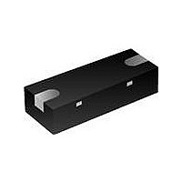
... General Information The CDDFN2-TxxC Series provides ESD and EFT protection for external ports of electronic devices such as cellular phones, hand held electronics and other portable electronic devices. The device measures 1. 0.65 mm and is available in a DFN-2 package and is intended to be mounted directly onto an FR4 printed circuit board. The device will fi 0402 footprint. ...

Page 2

... C (0.018-.022 DIMENSIONS: (INCHES) Recommended PCB Footprint C Typical Part Marking CDDFN2-T5.0C ............................................................................ E5 CDDFN2-T12C ............................................................................. E2 CDDFN2-T24C ............................................................................. E4 SIDE How to Order Common Diode Chip Diode Package DFN2 = DFN-2 Package Model Transient Voltage Suppressor Working Peak Reverse Voltage 5.0 = 5.0 V 12.0 = 12.0 V 24.0 = 24.0 V Suffi x ...

Page 3

... CDDFN2-TxxC Series - Surface Mount TVS Diode Rating & Characteristic Curves Pulse Waveform 120 Test Waveform Parameters µ 100 µ – Time (µs) Power Derating Curve Mounting on Glass Epoxy PCBs 100 Ambient Temperature (°C) Specifi cations are subject to change without notice. ...

Page 4

... CDDFN2-TxxC Series - Surface Mount TVS Diode Packaging Information The surface mount product is packaged tape and reel format per EIA-481 standard Index Hole Trailer Device ....... ....... ....... End ....... ....... ....... 10 pitches (min.) Item Symbol Carrier Width A Carrier Length B Carrier Depth C Sprocket Hole d Reel Outside Diameter D Reel Inner Diameter ...

Related keywords