CDDFN2-T3.3LC Bourns Inc., CDDFN2-T3.3LC Datasheet

TVS DIODE 3.3V BI SMD

CDDFN2-T3.3LC

Manufacturer Part Number
CDDFN2-T3.3LC
Description
TVS DIODE 3.3V BI SMD
Manufacturer
Bourns Inc.
Series
CDr
Datasheet

Specifications of CDDFN2-T3.3LC

Package / Case
2-UFDFN
Voltage - Reverse Standoff (typ)
3V
Voltage - Breakdown
4V
Polarization
Bidirectional
Mounting Type
Surface Mount
Polarity
Bidirectional
Channels
1 Channel
Clamping Voltage
5 V
Operating Voltage
+/- 3.8 V
Breakdown Voltage
4 V to 6.5 V
Termination Style
SMD/SMT
Peak Surge Current
5 A
Capacitance
13 pF
Maximum Operating Temperature
+ 125 C
Minimum Operating Temperature
- 55 C
Dimensions
0.55 mm W x 0.95 mm L x 0.45 mm H
Mounting Style
SMD/SMT
Reverse Stand-off Voltage Vrwm
3.3V
Clamping Voltage Vc Max
8V
Diode Configuration
Bidirectional
Peak Pulse Current Ippm
5A
Diode Case Style
DFN
No. Of Pins
2
Breakdown Voltage Vbr
6.5V
Breakdown Voltage Min
4V
Lead Free Status / RoHS Status
Lead free / RoHS Compliant
Power (watts)
-
Lead Free Status / Rohs Status
Lead free / RoHS Compliant
Other names
CDDFN2-T3.3LCTR

Available stocks

Company
Part Number
Manufacturer
Quantity
Price
Part Number:
CDDFN2-T3.3LC
Manufacturer:
BOURNS/伯恩斯
Quantity:
20 000
The Bourns
surge protection for external ports of electronic devices such as cellular phones,
handheld electronics and other portable electronic devices.
The device measures 1.0 mm x 0.60 mm x 0.55 mm and is available in a DFN-2
package and is intended to be mounted directly onto an FR4 printed circuit board.
The device will fi t a 0402 footprint.
The device is designed to meet IEC 61000-4-2 (ESD), IEC 61000-4-4 (EFT) and
IEC 61000-4-5 (Surge) protection requirements.
*RoHS Directive 2002/95/EC Jan 27, 2003 including Annex.
Specifi cations are subject to change without notice.
Customers should verify actual device performance in their specifi c applications.
Parameter
Operating Supply Voltage
Peak Pulse Current @ 8/20 μs
Operating Temperature
Storage Temperature
Parameter
Working Peak Voltage
Breakdown Voltage @ 1 mA
Leakage Current @ 5 V
Capacitance @ 0 V, 1 MHz
Clamping Voltage @ I P = 1 A 8/20 μs
Clamping Voltage @ I PP = 5 A 8/20 μs
ESD Protection per IEC 61000-4-2
EFT Protection per IEC 61000-4-4
@ 5/50 nS
EFT Protection per IEC 61000-4-5
@ 8/20 μS
General Information
Thermal Characteristics (@ T
Electrical Characteristics (@ T
Contact Discharge
Air Discharge
®
Model CDDFN2-T3.3LC low capacitance device provides ESD, EFT and
A
A
= 25 °C Unless Otherwise Noted)
Asia-Pacifi c: Tel: +886-2 2562-4117 • Fax: +886-2 2562-4116
Europe: Tel: +41-41 768 5555 • Fax: +41-41 768 5510
The Americas: Tel: +1-951 781-5500 • Fax: +1-951 781-5700
www.bourns.com
Symbol
Symbol
Features
CDDFN2-T3.3LC - Surface Mount TVS Diode
T OPR
Surge
T STG
V
V DC
V BR
ESD
ESD
EFT
I PP
C J
V C
V C
WM
Bidirectional TVS 3.3 V
Low capacitance - 13 pF
ESD protection >15 kV
Fits 0402 footprint
I L
Min.
Min.
-3.8
-55
-55
15
4
8
Typ.
Typ.
+25
+25
3.0
0.1
5.0
6.5
13
5
Applications
Computers and peripherals
Communication systems
Audio & video equipment
Portable instrumentation
Max.
Max.
+125
+150
16.5
3.8
3.3
6.5
1.0
6.5
50
8
5
Unit
Unit
μA
pF
ºC
ºC
kV
kV
A
V
V
V
V
A
A
V

Related parts for CDDFN2-T3.3LC

CDDFN2-T3.3LC Summary of contents

Page 1

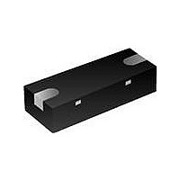
... General Information ® The Bourns Model CDDFN2-T3.3LC low capacitance device provides ESD, EFT and surge protection for external ports of electronic devices such as cellular phones, handheld electronics and other portable electronic devices. The device measures 1 0. 0.55 mm and is available in a DFN-2 package and is intended to be mounted directly onto an FR4 printed circuit board. ...

Page 2

... CDDFN2-T3.3LC - Surface Mount TVS Diode Product Dimensions This is a molded DFN-2 package with lead free 100 % Sn plating on the terminations. It weighs approximately 30 mg. TOP VIEW A SIDE VIEW D BOTTOM VIEW 45 ° 0.15 0.05 (0.006) (0.002) MM DIMENSIONS: (INCHES) Dimensions Symbol Min. Nom. 1.00 A (0.039) ...

Page 3

... CDDFN2-T3.3LC - Surface Mount TVS Diode Performance Graphs Pulse Waveform 120 Test Waveform Parameters µ 100 µ – Time (µs) Typical Capacitance Variation Input Voltage (V) Specifi cations are subject to change without notice. Customers should verify actual device performance in their specifi c applications. ...

Page 4

... CDDFN2-T3.3LC - Surface Mount TVS Diode Packaging Information The surface mount product is packaged tape and reel format per EIA-481 standard Index Hole Trailer Device ....... ....... ....... End ....... ....... ....... 10 pitches (min.) Item Symbol Carrier Width A Carrier Length B Carrier Depth C Sprocket Hole d Reel Outside Diameter D Reel Inner Diameter ...

Related keywords