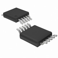
ISL23315TFUZ-T7A Intersil, ISL23315TFUZ-T7A Datasheet

ISL23315TFUZ-T7A
Specifications of ISL23315TFUZ-T7A
Available stocks
Related parts for ISL23315TFUZ-T7A
ISL23315TFUZ-T7A Summary of contents
Page 1
... FIGURE 2. V CAUTION: These devices are sensitive to electrostatic discharge; follow proper IC Handling Procedures. | 1-888-INTERSIL or 1-888-468-3774 Intersil (and design) and XDCP are trademarks owned by Intersil Corporation or one of its subsidiaries. All other trademarks mentioned are the property of their respective owners = 3.3V CC internally ...
Page 2
Block Diagram V LOGIC SCL SDA I/O A1 BLOCK A0 Pin Configurations ISL23315 (10 LD MSOP) TOP VIEW V 1 LOGIC SCL 2 SDA ISL23315 (10 LD µTQFN) TOP VIEW SCL 1 SDA 2 A0 ...
Page 3
... Ordering Information PART NUMBER (Note 5) PART MARKING ISL23315TFUZ (Notes 1, 3) 3315T ISL23315UFUZ (Notes 1, 3) 3315U ISL23315WFUZ (Notes 1, 3) 3315W ISL23315TFRUZ-T7A (Notes ISL23315TFRUZ-TK (Notes ISL23315UFRUZ-T7A (Notes ISL23315UFRUZ-TK (Notes ISL23315WFRUZ-T7A (Notes ISL23315WFRUZ-TK (Notes NOTES: 1. Add “-T*” suffix for Tape and Reel option. Please refer to 2 ...
Page 4
... Thermal Resistance (Typical MSOP Package (Notes µTQFN Package (Notes Maximum Junction Temperature (Plastic Package .+150°C Storage Temperature Range .-65°C to +150°C Pb-Free Reflow Profile . . . . . . . . . . . . . . . . . . . . . . . . . . . . . . . see link below http://www.intersil.com/pbfree/Pb-FreeReflow.asp Recommended Operating Conditions Temperature . . . . . . . . . . . . . . . . . . . . . . . . . . . . . . . . . . . . .-40°C to +125°C V Supply Voltage 1. Supply Voltage ...
Page 5
Analog Specifications V CC stated. Boldface limits apply over the operating temperature range, -40°C to +125°C. (Continued) SYMBOL PARAMETER VOLTAGE DIVIDER MODE ( RH; measured at RW, unloaded) CC INL Integral non-linearity, guaranteed (Note 13) monotonic ...
Page 6
Analog Specifications V CC stated. Boldface limits apply over the operating temperature range, -40°C to +125°C. (Continued) SYMBOL PARAMETER R Offset, wiper at 0 position offset (Note 16) TCR Resistance temperature coefficient (Note 19) Operating Specifications V stated. Boldface limits ...
Page 7
Operating Specifications V stated. Boldface limits apply over the operating temperature range, -40°C to +125°C. (Continued) SYMBOL PARAMETER tShdnRec DCP recall time from shutdown mode ramp rate CC, LOGIC CC , LOGIC Ramp (Note 21) Serial ...
Page 8
Serial Interface Specification SYMBOL PARAMETER t STOP Condition Set-up Time SU:STO t STOP Condition Hold Time for Read HD:STO or Write t Output Data Hold Time DH t SDA and SCL Rise Time R t SDA and SCL Fall Time ...
Page 9
Timing Diagrams SDA vs SCL Timing SCL t SU:STA t HD:STA SDA (INPUT TIMING) SDA (OUTPUT TIMING) A0 and A1 Pin Timing START SCL SDA A0, A1 Typical Performance Curves 0.4 0.2 0 -0.2 -0 100 TAP POSITION ...
Page 10
Typical Performance Curves 0.4 0.2 0 -0.2 -0 100 TAP POSITION (DECIMAL) FIGURE 5. 10k INL vs TAP POSITION, V 0.4 0.2 0 -0.2 -0 100 TAP POSITION (DECIMAL) FIGURE 7. 10k RDNL vs TAP POSITION, ...
Page 11
Typical Performance Curves 100 TAP POSITION (DECIMAL) FIGURE 11. 10k WIPER RESISTANCE vs TAP POSITION, V 300 250 200 150 100 115 TAP POSITION (DECIMAL) FIGURE ...
Page 12
Typical Performance Curves 115 TAP POSITION (DECIMAL) FIGURE 17. 100k TCv vs TAP POSITION 10mV/DIV 1µs/DIV FIGURE 19. WIPER DIGITAL FEED-THROUGH 1V/DIV 1µs/DIV SCL 9TH CLOCK OF THE DATA BYTE ...
Page 13
Typical Performance Curves CH1: 0.5V/DIV, 0.2µs/DIV RH PIN CH2: 0.2V/DIV, 0.2µs/DIV RW PIN R = 10k TOTAL -3dB FREQUENCY = 1.4MHz AT MIDDLE TAP FIGURE 23. 10k -3dB CUT OFF FREQUENCY Functional Pin Descriptions Potentiometers Pins RH AND RL The ...
Page 14
RW and RL increases monotonically, while the resistance between RH and RW decreases monotonically. While the ISL23315 is being powered up, the WR is reset to 80h (128 decimal), which locates RW roughly at the center between R ...
Page 15
SCL SDA START FIGURE 26. VALID DATA CHANGES, START AND STOP CONDITIONS SCL FROM MASTER SDA OUTPUT FROM TRANSMITTER HIGH IMPEDANCE SDA OUTPUT FROM RECEIVER START FIGURE 27. ACKNOWLEDGE RESPONSE FROM RECEIVER SIGNALS FROM THE MASTER SIGNAL AT SDA SIGNALS ...
Page 16
Write Operation A Write operation requires a START condition, followed by a valid Identification Byte, a valid Address Byte, a Data Byte, and a STOP condition. After each of the three bytes, the ISL23315 responds with an ACK. The data ...
Page 17
... Accordingly, the reader is cautioned to verify that data sheets are current before placing orders. Information furnished by Intersil is believed to be accurate and reliable. However, no responsibility is assumed by Intersil or its subsidiaries for its use; nor for any infringements of patents or other rights of third parties which may result from its use. No license is granted by implication or otherwise under any patent or patent rights of Intersil or its subsidiaries. ...
Page 18
Mini Small Outline Plastic Packages (MSOP -B- INDEX 1 2 0.20 (0.008) AREA TOP VIEW 0.25 (0.010) GAUGE PLANE SEATING PLANE - 0.10 (0.004) b -H- - 0.20 (0.008) SIDE VIEW 0.20 ...
Page 19
Package Outline Drawing L10.2.1x1.6A 10 LEAD ULTRA THIN QUAD FLAT NO-LEAD PLASTIC PACKAGE Rev 5, 3/10 2.10 B 0.10 2X TOP VIEW (10 X 0.20) (10X 0.60) (2.00) (0.80) (1.30) (6X 0.50 ) (2.50) TYPICAL RECOMMENDED LAND PATTERN 19 ISL23315 ...


