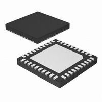
ISL41334IRZ-T7A Intersil, ISL41334IRZ-T7A Datasheet - Page 18

ISL41334IRZ-T7A
Manufacturer Part Number
ISL41334IRZ-T7A
Description
IC TXRX RS232/485 DL 2PRT 40QFN
Manufacturer
Intersil
Datasheet
1.ISL81334IAZ-T.pdf
(28 pages)
Specifications of ISL41334IRZ-T7A
Lead Free Status / RoHS Status
Lead free / RoHS Compliant
Available stocks
Company
Part Number
Manufacturer
Quantity
Price
Company:
Part Number:
ISL41334IRZ-T7A
Manufacturer:
Intersil
Quantity:
74
the logic device’s low V
powered dual protocol input. Connecting the V
power supply of the logic device (as shown in Figure 12)
limits the ISL41334’s Rx output V
and reduces the Tx and control input switching points to
values compatible with the logic device output levels.
Tailoring the logic pin input switching points and output levels
to the supply voltage of the UART, ASIC, or µcontroller
eliminates the need for a level shifter/translator between the
two ICs.
V
switching points may not provide enough noise margin when
V
various V
particular V
L
L
can be anywhere from V
< 1.8V. Table 5 indicates typical V
FIGURE 12. USING V
V
GND
GND
1.65V
1.8V
2.0V
2.5V
3.3V
L
TABLE 5. V
L
V
V
ISL81334
ISL41334
values so the user can ascertain whether or not a
CC
CC
L
(V)
voltage meets his needs.
= +5V
= +5V
R
R
D
D
V
A
Y
A
Y
L
IH
V
V
V
V
IH
IH
AND V
OH
OH
OH
L
≥ 2V
= 0.9V
PIN TO ADJUST LOGIC LEVELS
= 5V
= 2V
might not exceed the V
CC
V
V
18
IL
V
OH
OH
0.79
0.82
0.87
0.99
1.19
IH
down to 1.65V, but the input
vs V
≤ 2V
≤ 2V
(V)
OH
UART/PROCESSOR
UART/PROCESSOR
L
to V
IH
R
T
R
T
FOR V
XD
XD
XD
XD
V
V
and V
CC
CC
L
(see Figure 15),
= +2V
= +2V
CC
DIODE
DIODE
ESD
ESD
GND
GND
IL
L
= 5V
values for
pin to the
V
0.50
0.60
0.69
0.86
1.05
IL
IH
ISL81334, ISL41334
(V)
of a 5V
The V
shown in Figures 20 and 21. All of the DC V
to inputs with internal pull-up resistors (DE, SP, LB, ON/OFF)
being driven to the low input state. The worst case I
occurs during SHDN (see Figure 20), due to the I
the ON/OFF pin pull-up resistor when that pin is driven low.
I
Figure 20 drops by about 40µA (at V
SP inputs are high (middle vs top curve). I
RS-232 mode, because only the ON/OFF pin should be
driven low. When all these inputs are driven high, I
<1µA, so to minimize power dissipation drive these inputs
high when unneeded (e.g., SP inputs aren’t used in RS-232
mode, so drive them high).
Active Low Rx Enable (RXEN)
In many RS-485 applications, especially half duplex
configurations, users like to accomplish “echo cancellation”
by disabling the corresponding receiver while its driver is
transmitting data. This function is available on the QFN
package via an active low RXEN pin for each port. The
active low function also simplifies direction control, by
allowing a single Tx/Rx direction control line. If an active high
RXEN were used, either two valuable I/O pins would be
used for direction control, or an external inverter is required
between DE and RXEN. Figure 13 details the advantage of
using the RXEN pin.
IL
Tx/Rx
through an input pull-up resistor is ~20µA, so the I
FIGURE 13. USING ACTIVE LOW vs ACTIVE HIGH RX
L
ACTIVE LOW RX ENABLE
ACTIVE HIGH RX ENABLE
supply current (I
Tx/Rx
ENABLE
RXEN *
* QFN ONLY
DE
RXEN
RA
DY
DEN
RA
DY
ISL41334
L
) is typically less than 100µA, as
ISL81387
D
R
D
R
GND
+5V
V
B
A
Y
Z
CC
+5V
GND
V
B
A
Y
Z
CC
L
= 5V) when the two
L
is lowest in the
L
+
current is due
0.1µF
November 21, 2007
+
0.1µF
L
L
through
L
drops to
current
L
FN6202.3
in


