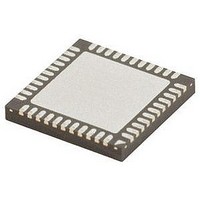
DS92LX2121SQE/NOPB National Semiconductor, DS92LX2121SQE/NOPB Datasheet - Page 4

DS92LX2121SQE/NOPB
Manufacturer Part Number
DS92LX2121SQE/NOPB
Description
IC SER/DESER 10-50MHZ 40-LLP
Manufacturer
National Semiconductor
Datasheet
1.DS92LX2121SQXNOPB.pdf
(38 pages)
Specifications of DS92LX2121SQE/NOPB
Serdes Function
Serializer
Data Rate
100Kbps
Ic Output Type
CML
No. Of Inputs
21
No. Of Outputs
2
Supply Voltage Range
3V To 3.6V
Driver Case Style
LLP
No. Of Pins
40
Msl
MSL 3 - 168 Hours
Rohs Compliant
Yes
Leaded Process Compatible
Yes
Lead Free Status / RoHS Status
Lead free / RoHS Compliant
Other names
DS92LX2121SQE/NOPBTR
www.national.com
LVCMOS PARALLEL INTERFACE
DIN[20:0]
PCLK
GENERAL PURPOSE OUTPUT (GPO)
GPO[3:0]
SERIAL CONTROL BUS - I
SCL
SDA
M/S
CAD
CONTROL AND CONFIGURATION
PDB
RES
Channel Link III INTERFACE
DOUT+
DOUT-
Power and Ground
VDDPLL
VDDT
VDDCML
VDDD
VDDIO
VSS
DS92LX2121 Serializer Pin Descriptions
Pin Name
5, 4, 3, 2, 1, 40,
39, 38, 37, 36,
35, 33, 32, 30,
29, 28, 27, 26,
22, 21, 20, 19
25, 24, 23
Pin No.
10, 11
DAP
12
13
17
16
14
15
18
34
31
6
7
8
9
2
C COMPATIBLE
Input, LVCMOS w/
pull down
Input, analog
Inputs, LVCMOS w/
Input/Output, Open
Input/Output, Open
Input, LVCMOS w/
Input, LVCMOS w/
Input, LVCMOS w/
Input/Output, CML
Input/Output, CML
Output, LVCMOS
Power, Analog
Power, Analog
Power, Analog
Power, Digital
Power, Digital
Ground, DAP
I/O, Type
pull down
pull down
pull down
pull down
Drain
Drain
Parallel data inputs.
Pixel Clock Input Pin. Strobe edge set by TRFB configuration.
General-purpose pins individually configured as outputs; which are used to
control and respond to various commands.
Clock line for the serial control bus communication
SCL requires an external pull-up resistor to V
Data line for the serial control bus communication
SDA requires an external pull-up resistor to V
I
M/S = L, Master mode (default); device generates and drives the SCL clock
line. Device is connected to a slave peripheral on the bus. (Serializer initially
starts up in Standby mode and is enabled through remote wakeup by the
Deserializer)
M/S = H, Slave; device accepts SCL clock input
Continuous Address Decoder
Input pin to select the Slave Device Address.
Input is connect to external resistor divider to programmable Device ID
address (see Serial Control Bus Connection).
Power down Mode Input Pin.
PDB = H, Transmitter is enabled and is ON.
PDB = L, Transmitter is in Sleep (Power Down). When the transmitter is in
the SLEEP state, the PLL is shutdown, and IDD is minimized.
Reserved. This pin MUST be tied LOW.
Non-inverting differential output, back-channel input.
Inverting differential output, back-channel input.
PLL Power, 1.8V ±5%
Tx Analog Power, 1.8V ±5%
LVDS & BC Dr Power, 1.8V ±5%
Digital Power, 1.8V ±5%
Power for input stage, The single-ended inputs are powered from V
DAP must be grounded. Connect to the ground plane (GND) with at least 16
vias.
2
C Mode Select
4
Description
DDIO
DDIO
.
.
DDIO
.


