LS027B7DH01 Sharp Microelectronics, LS027B7DH01 Datasheet - Page 14
LS027B7DH01
Manufacturer Part Number
LS027B7DH01
Description
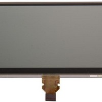
LCD Graphic Display Modules & Accessories 2.7 WQVGA HR-TFT 400x240 w/FPC
Manufacturer
Sharp Microelectronics
Datasheet
1.LS027B7DH01.pdf
(32 pages)
Specifications of LS027B7DH01
Pixel Density
400 x 240
Module Size (w X H X T)
62.8 mm x 42.82 mm
Viewing Area (w X H)
58.8 mm x 35.28 mm
Operating Temperature Range
- 20 C to + 70 C
Attached Touch Screen
No
Product
2.7 in WQVGA Monochrome
Display Mode
Transmissive
Interface
Serial
Lead Free Status / RoHS Status
Lead free / RoHS Compliant
Available stocks
Company
Part Number
Manufacturer
Quantity
Price
Company:

Part Number:
LS027B7DH01
Manufacturer:
SAMSUNG
Quantity:
1 000
Company:
Part Number:
LS027B7DH01A
Manufacturer:
SHARP
Quantity:
1 000


6-2) Power Supply Sequence
VDD/VDDA(5V)
DISP
EXTCOMIN
SCS
Others
【Remark】 Cautions when powering on
※Refer to timing chart and AC timing characteristics for detail
※1 ③ and ④ may be opposite (however, TCOM polarity inversion will not occur even with EXTCOMIN between
DISP=”L”. Also, when DISP and EXTCOMIN are simultaneously started up, allow 30us or more before SCS
starts up (It may be less than 60us).
※2 Setting value for pixel memory initialization
SCS=Driving accordingly to clear pixel internal memory method (use all clear flag or write all screen white)
S1=M2 (all clear flag) = “H” or write white
SCLK: Normal Driving
Remark 1) VDD and VDDA should rise simultaneously or VDD should rise first.
Remark 2) VDD and VDDA shouldl simultaneously or VDD should fall first
[ON Sequence]
(1) 5V rise time (depends on IC)
(2) Pixel memory initialization T2: 1V or more Initialize with M2 (all clear flag) or write all screen white
(3) Release time for initialization of TCOM latch
(4) TCOM polarity initialization time
[Normal Operation]
Duration of normal driving
[Off Sequence]
(5) Pixel memory initialization time
(6) VA, VB, VCOM initialization time
(7) 5V falling time (Depends on IC)
Time required to release COM related latch circuit initialization which is initializing using DISP signals
Time required initializing TCOM polarity accordingly to EXTCOMIN input
GND
GND
GND
GND
GND
①
T1
※2
※2
On Sequence
②
T2
③※1 ④※1
T3
T4
SPEC No.
LCY-1210401A
Normal operation
Normal operation
Normal operation
Normal operation
T5: 1V or more
T6: 1V or more
T4: 30us or more
T3: 30us or more
※2
※2
⑤
T5
MODEL No.
Off sequence
LS027B7DH01
⑥
T6
⑦
T7
GND
GND
GND
GND
GND
PAGE
11
Related parts for LS027B7DH01
Image
Part Number
Description
Manufacturer
Datasheet
Request
R


Part Number:
Description:
SENSOR LEVEL FLOAT M10
Manufacturer:
MEDER electronic
Datasheet:

Part Number:
Description:
Ls02 Level Sensors
Manufacturer:
MEDER electronic Inc.
Datasheet:

Part Number:
Description:
REED LEVEL SENSOR
Manufacturer:
MEDER electronic
Datasheet:
Part Number:
Description:
REED LEVEL SENSOR
Manufacturer:
MEDER electronic
Datasheet:

Part Number:
Description:
Level Sensors With Magnetic Floats
Manufacturer:
MEDER electronic Inc.
Datasheet:
Part Number:
Description:
Reed Switch Or Relay From Meder
Manufacturer:
MEDER electronic Inc.
Datasheet:
Part Number:
Description:
Reed Switch Or Relay From Meder
Manufacturer:
MEDER electronic Inc.
Datasheet:
Part Number:
Description:
LS Level Sensor
Manufacturer:
MEDER [Meder Electronic]
Datasheet:

Part Number:
Description:
IC FLASH 32MBIT 110NS 56SSOP
Manufacturer:
Sharp Microelectronics
Datasheet:

Part Number:
Description:
IC FLASH 16MBIT 100NS 56TSOP
Manufacturer:
Sharp Microelectronics
Datasheet:

Part Number:
Description:
IC FLASH 64MBIT 120NS 56TSOP
Manufacturer:
Sharp Microelectronics
Datasheet:

Part Number:
Description:
IC FLASH 16MBIT 90NS 48TSOP
Manufacturer:
Sharp Microelectronics
Datasheet:
Part Number:
Description:
IC SRAM 16KBIT 100NS 24DIP
Manufacturer:
Sharp Microelectronics
Datasheet: