UM245R FTDI, UM245R Datasheet - Page 6
UM245R
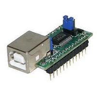
Manufacturer Part Number
UM245R
Description
Interface Modules & Development Tools USB to Parallel FIFO Dev Mod for FT245R
Manufacturer
FTDI
Type
Development Moduler
Datasheet
1.UM245R.pdf
(27 pages)
Specifications of UM245R
Interface Type
USB, Parallel FIFO
Data Bus Width
8 bit
Operating Supply Voltage
1.8 V to 5.25 V
Product
Interface Modules
Supported Devices
FT245R
Svhc
No SVHC (18-Jun-2010)
Development Tool Type
Development Kit
Kit Features
Single Chip USB To Parallel FIFO Bidirectional Data Transfer Interface
Rohs Compliant
Yes
Mcu Supported Families
FT245RL
Supported Families
FT245RL
Tool / Board Applications
USB To Parallel FIFO Interface
For Use With/related Products
FT245R
Lead Free Status / RoHS Status
Lead free / RoHS Compliant


Document Reference No.: FT_000202
UM245R USB - Parallel FIFO Development Module Datasheet Version 1.04
Clearance No.: FTDI# 124
3
FT245RL Features and Enhancement
3.1 Key Features
This section summarises the key features and enhancements of the FT245R IC device which is used
in the UM245R Module. For further details, consult the FT245R datasheet, which is available from
the
FTDI
website.
Integrated Clock Circuit – Previous generations of FTDI‟s USB to parallel FIFO interface devices
required an external crystal or ceramic resonator. The clock circuit has now been integrated onto
the device meaning that no crystal or ceramic resonator is required. It is important to note that
VCC must be between 4.0 and 5.25V. However, if required, an external 12MHz crystal can be used
as the clock source.
Integrated EEPROM – Previous generations of FTDI‟s USB to parallel FIFO interface devices
required an external EEPROM if the device were to use USB Vendor ID (VID), Product ID (PID),
serial number and product description strings other than the default values in the device itself. This
external EEPROM has now been integrated onto the FT245R chip meaning that all designs have the
option to change the product description strings. A user area of the internal EEPROM is available for
storing additional data. The internal EEPROM is programmable in circuit, over USB without any
additional voltage requirement.
Pre-programmed EEPROM – The FT245R is supplied with its internal EEPROM pre-programmed
with a serial number which is unique to each individual device. This, in most cases, will remove the
need to program the device EEPROM.
Integrated USB Resistors – Previous generations of FTDI‟s USB to parallel FIFO interface devices
required two external series termination resistors on the USBDP and USBDM signals, and a 1.5 kΩ
pull up resistor on USBDP. These three resistors have now been integrated onto the device.
Integrated AVCC Filtering – Previous generations of FTDI‟s USB to parallel FIFO interface devices
had a separate AVCC pin – the supply to the internal PLL. This pin required an external R-C filter.
The separate AVCC pin is now connected internally to VCC, and the filter has now been integrated
onto the chip.
Fewer External Components – Integration of the crystal, EEPROM, USB resistors, and AVCC filter
will substantially reduce the bill of materials cost for USB interface designs using the FT245R
compared to its FT245BM predecessor.
Enhanced Asynchronous Bit Bang Mode with RD# and WR# Strobes – The FT245R supports
FTDI‟s BM chip bit bang mode. In bit bang mode, the eight parallel FIFO data bus lines can be
switched from the regular interface mode to an 8-bit general purpose I/O port. Data packets can be
sent to the device and they will be sequentially sent to the interface at a rate controlled by an
internal timer (equivalent to the baud rate prescaler). With the FT245R device this mode has been
enhanced so that the internal RD# and WR strobes are now brought out of the device which can be
used to allow external logic to be clocked by accesses to the bit bang I/O bus. This option is
described more fully in a application note AN232R-01,
Bit Bang Modes for the FT232R and
FT245R.
Synchronous Bit Bang Mode – Synchronous bit bang mode differs from asynchronous bit bang
mode in that the interface pins are only read when the device is written to. This makes it easier for
the controlling program to measure the response to an output stimulus as the data returned is
synchronous to the output data. The feature was previously seen in FTDI‟s FT2232D device. This
option is described more fully in a application note AN232R-01,
Bit Bang Modes for the FT232R and
FT245R.
Lower Supply Voltage – Previous generations of the chip required 5V supply on the VCC pin. The
FT245R will work with a VCC supply in the range 4.0V - 5V. Bus powered designs would still take
their supply from the 5V on the USB bus. Self-powered designs must provide between 4.0V and
5.25V to VCC.
Integrated Level Converter on FIFO Interface and Control Signals – VCCIO pin supply can
be from 1.8V to 5V. Connecting the VCCIO pin to 1.8V, 2.8V, or 3.3V allows the device to directly
interface to 1.8V, 2.8V or 3.3V and other logic families without the need for external level converter
ICs.
© Copyright 2009 Future Technology Devices International Ltd
5
Related parts for UM245R
Image
Part Number
Description
Manufacturer
Datasheet
Request
R

Part Number:
Description:
Interface Modules & Development Tools USB to Serial UART MiniB Dev Mod FT232R
Manufacturer:
FTDI
Datasheet:

Part Number:
Description:
BOARD, EVALUATION, EU PSU
Manufacturer:
FTDI
Datasheet:
Part Number:
Description:
BOARD, EVALUATION, UK PSU
Manufacturer:
FTDI
Datasheet:
Part Number:
Description:
BOARD, EVALUATION, US PSU
Manufacturer:
FTDI
Datasheet:
Part Number:
Description:
Specifications: Manufacturer: FTDI ; Product Category: USB Interface IC ; RoHS: Details ; Operating Supply Voltage: 3 V to 5.25 V ; Supply Current: 25 mA ; Maximum Operating Temperature: + 70 C ; Mounting Style: SMD/SMT ; Package / Case: QFN-32
Manufacturer:
FTDI
Part Number:
Description:
integr. usb2.0/uart lqfp32 rohs ftdi reel c1k...
Manufacturer:
FTDI
Datasheet:
Part Number:
Description:
Interface Development Tools USB to UART Breakout Board
Manufacturer:
FTDI
Datasheet:

Part Number:
Description:
IC USB TO SERIAL UART 32-QFN
Manufacturer:
FTDI, Future Technology Devices International Ltd

Part Number:
Description:
USB Interface IC USB to Serial UART Enhanced IC SSOP-28
Manufacturer:
FTDI
Datasheet:

Part Number:
Description:
IC, USB UART INTERFACE, SSOP-28
Manufacturer:
FTDI
Datasheet:

Part Number:
Description:
IC, USB UART INTERFACE, QFN-32
Manufacturer:
FTDI
Datasheet:
Part Number:
Description:
IC, USB FIFO INTERFACE, SSOP-28
Manufacturer:
FTDI
Datasheet:
Part Number:
Description:
MODULE, USB, 4 PORT, FT4232H BASED
Manufacturer:
FTDI
Datasheet:
Part Number:
Description:
357-036-542-201 CARDEDGE 36POS DL .156 BLK LOPRO
Manufacturer:
FTDI
Datasheet:
Part Number:
Description:
357-036-542-201 CARDEDGE 36POS DL .156 BLK LOPRO
Manufacturer:
FTDI
Datasheet: