TWR-S08MM128-KIT Freescale Semiconductor, TWR-S08MM128-KIT Datasheet - Page 16
TWR-S08MM128-KIT
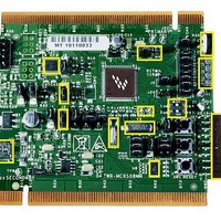
Manufacturer Part Number
TWR-S08MM128-KIT
Description
MCU, MPU & DSP Development Tools For 9S08MM128 USB CAN
Manufacturer
Freescale Semiconductor
Datasheet
1.MC9S08MM128CMB.pdf
(52 pages)
Specifications of TWR-S08MM128-KIT
Processor To Be Evaluated
9S08MM128
Data Bus Width
8 bit
Interface Type
USB, CAN
Silicon Manufacturer
Freescale
Core Architecture
Coldfire, HCS08
Core Sub-architecture
Coldfire V1, HCS08
Silicon Core Number
MCF51, MC9S08
Silicon Family Name
Flexis - MCF51MM, Flexis - S08MM
Rohs Compliant
Yes
Lead Free Status / RoHS Status
Lead free / RoHS Compliant


Electrical Characteristics
For most applications, P
is:
Solving
where K is a constant pertaining to the particular part. K can be determined from
for a known T
for any value of T
2.4
Although damage from static discharge is much less common on these devices than on early CMOS circuits, normal handling
precautions should be used to avoid exposure to static discharge. Qualification tests are performed to ensure that these devices
can withstand exposure to reasonable levels of static without suffering any permanent damage.
All ESD testing is in conformity with CDF-AEC-Q00 Stress Test Qualification for Automotive Grade Integrated Circuits.
(http://www.aecouncil.com/) This device was qualified to AEC-Q100 Rev E.
A device is considered to have failed if, after exposure to ESD pulses, the device no longer meets the device specification
requirements. Complete dc parametric and functional testing is performed per the applicable device specification at room
temperature followed by hot temperature, unless specified otherwise in the device specification.
16
Freescale reserves the right to change the detail specifications as may be required to permit improvements in the design of its products.
#
1
2
3
4
Equation 1
Human Body
Machine
Latch-up
ESD Protection Characteristics
Human Body Model (HBM)
Machine Model (MM)
Charge Device Model (CDM)
Latch-up Current at T
A
Model
. Using this value of K, the values of P
A
.
and
I/O
Equation 2
P
Series Resistance
Storage Capacitance
Number of Pulse per pin
Series Resistance
Storage Capacitance
Number of Pulse per pin
Minimum input voltage limit
Maximum input voltage limit
Table 8. ESD and Latch-Up Protection Characteristics
int
A
and can be neglected. An approximate relationship between P
Rating
= 125C
for K gives:
Table 7. ESD and Latch-up Test Conditions
K = P
D
P
Description
(T
D
= K (T
A
D
+ 273C) +
and T
J
J
+ 273C)
can be obtained by solving
Symbol
JA
V
V
V
I
HBM
CDM
LAT
MM
(P
D
)
2
Equation 3
2000
200
500
00
Min
Symbol
R1
R1
—
—
—
—
C
C
Equation 1
by measuring P
D
Max
—
—
—
—
and T
Value
1500
–2.5
100
200
and
7.5
Freescale Semiconductor
3
0
3
J
Equation 2
(if P
D
Unit
mA
V
V
V
I/O
(at equilibrium)
Unit
pF
pF
—
—
V
V
is neglected)
iteratively
C
T
T
T
T
Eqn. 2
Eqn. 3
Related parts for TWR-S08MM128-KIT
Image
Part Number
Description
Manufacturer
Datasheet
Request
R

Part Number:
Description:
TOWER SYSTEM BOARD MC9S08MM128
Manufacturer:
Freescale Semiconductor
Datasheet:

Part Number:
Description:
Development Boards & Kits - S08 / S12 S08PT60 Tower Kit
Manufacturer:
Freescale Semiconductor
Datasheet:
Part Number:
Description:
Development Boards & Kits - S08 / S12 S08PT60Tower MCU mod
Manufacturer:
Freescale Semiconductor
Datasheet:
Part Number:
Description:
TOWER UNIVERSAL RS08/S08
Manufacturer:
Freescale Semiconductor
Datasheet:

Part Number:
Description:
Manufacturer:
Freescale Semiconductor, Inc
Datasheet:
Part Number:
Description:
Manufacturer:
Freescale Semiconductor, Inc
Datasheet:
Part Number:
Description:
Manufacturer:
Freescale Semiconductor, Inc
Datasheet:
Part Number:
Description:
Manufacturer:
Freescale Semiconductor, Inc
Datasheet:
Part Number:
Description:
Manufacturer:
Freescale Semiconductor, Inc
Datasheet:
Part Number:
Description:
Manufacturer:
Freescale Semiconductor, Inc
Datasheet:
Part Number:
Description:
Manufacturer:
Freescale Semiconductor, Inc
Datasheet:
Part Number:
Description:
Manufacturer:
Freescale Semiconductor, Inc
Datasheet:
Part Number:
Description:
Manufacturer:
Freescale Semiconductor, Inc
Datasheet:
Part Number:
Description:
Manufacturer:
Freescale Semiconductor, Inc
Datasheet:
Part Number:
Description:
Manufacturer:
Freescale Semiconductor, Inc
Datasheet: