M1AFS-ADV-DEV-KIT-PWR Actel, M1AFS-ADV-DEV-KIT-PWR Datasheet - Page 40
M1AFS-ADV-DEV-KIT-PWR
Manufacturer Part Number
M1AFS-ADV-DEV-KIT-PWR
Description
MCU, MPU & DSP Development Tools Fusion Advanced Dev Kit w/ Power
Manufacturer
Actel
Datasheet
1.M1AFS-ADV-DEV-KIT-PWR.pdf
(94 pages)
Specifications of M1AFS-ADV-DEV-KIT-PWR
Processor To Be Evaluated
M1AFS1500-FGG484
Interface Type
Ethernet, USB, I2C, UART
Operating Supply Voltage
1.5 V to 5 V
Lead Free Status / RoHS Status
Lead free / RoHS Compliant


Hardware Components
Low-Cost Programming Stick
40
Note:
The LCPS supplied with this kit is intended for use with the Fusion Advanced Development Kit. An LCPS supplied for other kits, although
electrically and functionally equivalent, may not connect seamlessly with the Fusion Advanced Development Kit board.
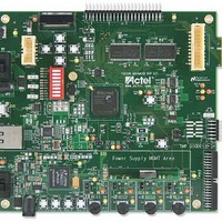
The Fusion Advanced Development Kit board can be programmed using the low-cost programming stick (LCPS). The
LCPS is a special version of the FlashPro3 programming circuitry that is compatible with FlashPro3 and the generic
FlashPro programming software
The LCPS, like this Fusion Advanced Development Kit board, is RoHS-compliant and is completely lead (Pb) free. To
use the LCPS with the FlashPro software, select the FlashPro3 from the list of programmer types. The LCPS behaves
exactly as if it were a regular encased FlashPro3 programmer. The 12-pin female connector socket is designed to
interface to the 12-pin right-angle male header on the Fusion Advanced Development Kit board.
You do not need to have the LCPS connected to the Fusion Advanced Development Kit board to operate once the
FPGA has been programmed. The Fusion Advanced Development Kit board requires the LCPS connected only during
programming.
The LCPS programs the FPGA through the JTAG pins. Fusion devices have a separate bank for the dedicated JTAG
pins. The JTAG pins can be run at any voltage from 1.5 V to 3.3 V (nominal). V
state machine to operate, even if the device is in bypass mode; V
Fusion part must be supplied to allow JTAG signals to transition the Fusion device. Isolating the JTAG power supply in
a separate I/O bank gives greater flexibility with supply selection and simplifies power supply and PCB design. If the
JTAG interface is neither used nor planned for use, the V
Figure 2-35 · Low-Cost Programming Stick
(Figure
2-35).
JTAG
pin together with the TRST pin could be tied to GND.
JTAG
Fusion Advanced Development Kit User’s Guide
alone is insufficient. Both V
CC
must also be powered for the JTAG
JTAG
and V
CC
to the
Related parts for M1AFS-ADV-DEV-KIT-PWR
Image
Part Number
Description
Manufacturer
Datasheet
Request
R

Part Number:
Description:
MCU, MPU & DSP Development Tools Fusion Advanced Development Kit
Manufacturer:
Actel
Part Number:
Description:
MCU, MPU & DSP Development Tools Silicon Sculptor Programming Mod
Manufacturer:
Actel
Part Number:
Description:
MCU, MPU & DSP Development Tools InSystem Programming ProASICPLUS Devices
Manufacturer:
Actel
Part Number:
Description:
Programming Socket Adapters & Emulators PQ160 Module
Manufacturer:
Actel
Part Number:
Description:
Programming Socket Adapters & Emulators Axcelerator Adap Module Kit
Manufacturer:
Actel
Part Number:
Description:
Programming Socket Adapters & Emulators Evaluation
Manufacturer:
Actel
Part Number:
Description:
Programming Socket Adapters & Emulators AFDX Solutions
Manufacturer:
Actel
Part Number:
Description:
Programming Socket Adapters & Emulators SILICON SCULPTOR ADAPTER MODULE
Manufacturer:
Actel
Datasheet:
Part Number:
Description:
Programming Socket Adapters & Emulators Axcelerator Adap Module Kit
Manufacturer:
Actel
Part Number:
Description:
Programming Socket Adapters & Emulators Evaluation
Manufacturer:
Actel
Part Number:
Description:
Programming Socket Adapters & Emulators Silicon Sculptor Software
Manufacturer:
Actel
Part Number:
Description:
Programming Socket Adapters & Emulators InSystem Programming ProASICPLUS Devices
Manufacturer:
Actel
Part Number:
Description:
Programming Socket Adapters & Emulators Evaluation
Manufacturer:
Actel
Part Number:
Description:
Programming Socket Adapters & Emulators Axcelerator Adap Module Kit
Manufacturer:
Actel
Part Number:
Description:
Programming Socket Adapters & Emulators Axcelerator Adap Module Kit
Manufacturer:
Actel