OM11049,598 NXP Semiconductors, OM11049,598 Datasheet - Page 17
OM11049,598
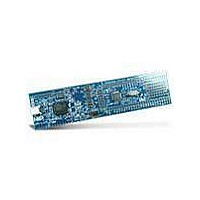
Manufacturer Part Number
OM11049,598
Description
MCU, MPU & DSP Development Tools LPC1114 Demo Boards Cortex M0
Manufacturer
NXP Semiconductors
Datasheet
1.OM11049598.pdf
(66 pages)
Specifications of OM11049,598
Processor To Be Evaluated
LPC1114
Processor Series
LPC11xx
Interface Type
I2C, SPI
Maximum Operating Temperature
+ 85 C
Minimum Operating Temperature
- 40 C
Operating Supply Voltage
3.3 V
Tool Type
Demonstration Board
Core Architecture
ARM
Cpu Core
ARM Cortex M0
Data Bus Width
32 bit
Lead Free Status / RoHS Status
Lead free / RoHS Compliant


NXP Semiconductors
Table 5.
LPC1111_12_13_14
Product data sheet
Symbol
PIO0_5/SDA
PIO0_6/SCK0
PIO0_7/CTS
PIO0_8/MISO0/
CT16B0_MAT0
PIO0_9/MOSI0/
CT16B0_MAT1
SWCLK/PIO0_10/
SCK0/
CT16B0_MAT2
R/PIO0_11/AD0/
CT32B0_MAT3
PIO1_0 to PIO1_11
R/PIO1_0/AD1/
CT32B1_CAP0
R/PIO1_1/AD2/
CT32B1_MAT0
R/PIO1_2/AD3/
CT32B1_MAT1
LPC1111/12/13/14 pin description table (HVQFN33 package)
Pin
11
15
16
17
18
19
21
22
23
24
[4]
[3]
[3]
[3]
[3]
[3]
[5]
[5]
[5]
[5]
Start
logic
input
yes
yes
yes
yes
yes
yes
yes
yes
no
no
Type Reset
I/O
I/O
I/O
I/O
I/O
I
I/O
I/O
O
I/O
I/O
O
I
I/O
I/O
O
-
I/O
I
O
-
I/O
I
I
-
I/O
I
O
-
I/O
I
O
All information provided in this document is subject to legal disclaimers.
state
[1]
I;PU
-
I;PU
-
I;PU
-
I;PU
-
-
I;PU
-
-
I;PU
-
-
-
I;PU
-
-
-
I;PU
-
-
-
I;PU
-
-
-
I;PU
-
-
-
Rev. 4 — 10 February 2011
Description
PIO0_5 — General purpose digital input/output pin (open-drain).
SDA — I
I
PIO0_6 — General purpose digital input/output pin.
SCK0 — Serial clock for SPI0.
PIO0_7 — General purpose digital input/output pin (high-current
output driver).
CTS — Clear To Send input for UART.
PIO0_8 — General purpose digital input/output pin.
MISO0 — Master In Slave Out for SPI0.
CT16B0_MAT0 — Match output 0 for 16-bit timer 0.
PIO0_9 — General purpose digital input/output pin.
MOSI0 — Master Out Slave In for SPI0.
CT16B0_MAT1 — Match output 1 for 16-bit timer 0.
SWCLK — Serial wire clock.
PIO0_10 — General purpose digital input/output pin.
SCK0 — Serial clock for SPI0.
CT16B0_MAT2 — Match output 2 for 16-bit timer 0.
R — Reserved. Configure for an alternate function in the IOCONFIG
block.
PIO0_11 — General purpose digital input/output pin.
AD0 — A/D converter, input 0.
CT32B0_MAT3 — Match output 3 for 32-bit timer 0.
Port 1 — Port 1 is a 12-bit I/O port with individual direction and
function controls for each bit. The operation of port 1 pins depends on
the function selected through the IOCONFIG register block.
R — Reserved. Configure for an alternate function in the IOCONFIG
block.
PIO1_0 — General purpose digital input/output pin.
AD1 — A/D converter, input 1.
CT32B1_CAP0 — Capture input 0 for 32-bit timer 1.
R — Reserved. Configure for an alternate function in the IOCONFIG
block.
PIO1_1 — General purpose digital input/output pin.
AD2 — A/D converter, input 2.
CT32B1_MAT0 — Match output 0 for 32-bit timer 1.
R — Reserved. Configure for an alternate function in the IOCONFIG
block.
PIO1_2 — General purpose digital input/output pin.
AD3 — A/D converter, input 3.
CT32B1_MAT1 — Match output 1 for 32-bit timer 1.
2
C Fast-mode Plus is selected in the I/O configuration register.
2
C-bus, open-drain data input/output. High-current sink only if
…continued
32-bit ARM Cortex-M0 microcontroller
LPC1111/12/13/14
© NXP B.V. 2011. All rights reserved.
17 of 66
Related parts for OM11049,598
Image
Part Number
Description
Manufacturer
Datasheet
Request
R

Part Number:
Description:
NXP Semiconductors designed the LPC2420/2460 microcontroller around a 16-bit/32-bitARM7TDMI-S CPU core with real-time debug interfaces that include both JTAG andembedded trace
Manufacturer:
NXP Semiconductors
Datasheet:

Part Number:
Description:
NXP Semiconductors designed the LPC2458 microcontroller around a 16-bit/32-bitARM7TDMI-S CPU core with real-time debug interfaces that include both JTAG andembedded trace
Manufacturer:
NXP Semiconductors
Datasheet:
Part Number:
Description:
NXP Semiconductors designed the LPC2468 microcontroller around a 16-bit/32-bitARM7TDMI-S CPU core with real-time debug interfaces that include both JTAG andembedded trace
Manufacturer:
NXP Semiconductors
Datasheet:
Part Number:
Description:
NXP Semiconductors designed the LPC2470 microcontroller, powered by theARM7TDMI-S core, to be a highly integrated microcontroller for a wide range ofapplications that require advanced communications and high quality graphic displays
Manufacturer:
NXP Semiconductors
Datasheet:
Part Number:
Description:
NXP Semiconductors designed the LPC2478 microcontroller, powered by theARM7TDMI-S core, to be a highly integrated microcontroller for a wide range ofapplications that require advanced communications and high quality graphic displays
Manufacturer:
NXP Semiconductors
Datasheet:
Part Number:
Description:
The Philips Semiconductors XA (eXtended Architecture) family of 16-bit single-chip microcontrollers is powerful enough to easily handle the requirements of high performance embedded applications, yet inexpensive enough to compete in the market for hi
Manufacturer:
NXP Semiconductors
Datasheet:
Part Number:
Description:
The XA-S3 device is a member of Philips Semiconductors? XA(eXtended Architecture) family of high performance 16-bitsingle-chip microcontrollers
Manufacturer:
NXP Semiconductors
Datasheet:

Part Number:
Description:
The NXP BlueStreak LH75401/LH75411 family consists of two low-cost 16/32-bit System-on-Chip (SoC) devices
Manufacturer:
NXP Semiconductors
Datasheet:
Part Number:
Description:
The NXP LPC3130/3131 combine an 180 MHz ARM926EJ-S CPU core, high-speed USB2
Manufacturer:
NXP Semiconductors
Datasheet:
Part Number:
Description:
The NXP LPC3141 combine a 270 MHz ARM926EJ-S CPU core, High-speed USB 2
Manufacturer:
NXP Semiconductors
Part Number:
Description:
The NXP LPC3143 combine a 270 MHz ARM926EJ-S CPU core, High-speed USB 2
Manufacturer:
NXP Semiconductors

Part Number:
Description:
The NXP LPC3152 combines an 180 MHz ARM926EJ-S CPU core, High-speed USB 2
Manufacturer:
NXP Semiconductors
Part Number:
Description:
The NXP LPC3154 combines an 180 MHz ARM926EJ-S CPU core, High-speed USB 2
Manufacturer:
NXP Semiconductors

Part Number:
Description:
Standard level N-channel enhancement mode Field-Effect Transistor (FET) in a plastic package using NXP High-Performance Automotive (HPA) TrenchMOS technology
Manufacturer:
NXP Semiconductors
Datasheet: