OM11055,598 NXP Semiconductors, OM11055,598 Datasheet - Page 7
OM11055,598
Manufacturer Part Number
OM11055,598
Description
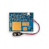
Capacitance Touch Sensor Development Tools PCF8883 Demo Board
Manufacturer
NXP Semiconductors
Datasheet
1.OM11055.pdf
(11 pages)
Specifications of OM11055,598
Interface Type
USB
Operating Voltage
9 V
Maximum Operating Temperature
+ 85 C
Minimum Operating Temperature
- 40 C
Operating Current
2.2 uA
For Use With/related Products
PCF8883
Lead Free Status / RoHS Status
Lead free / RoHS Compliant
Other names
63598 909 9352


NXP Semiconductors
5. Sensor adjustment
UM10370_2
User manual
4.3 Power supply options
4.4 High impedance op-amp
Power to the OM11055 PCB can be supplied using a mini USB cable (provided) or a 9V
battery. The 9V battery connector can be removed and a user provided power supply
could be connected at JP3 & JP4 for evaluation of a specific application. Using an
external power supply also allows for easy measuring of the power consumption.
Warning: There is no protection against reverse polarity of the external power supply.
A high input impedance rail-to-rail input and output op-amp (U2) is included on the board
to measure the voltage at the CPC pin of the PCF8883. A capacitor is connected
between pin CPC and Vss. The value of this capacitor is used to adjust the sensitivity of
the switch. Since this is a very high impedance node, measuring directly with a probe
would disturb the control loop. Therefore this voltage buffer has been included on the
board. By default, this op-amp is not connected, as it would add to power consumption
measurements. To enable U2, install two pin headers and jumpers at J12 and J16.
Remark 1: Always first provide power to op-amp U2 (jumper J12) before connecting the
input to pin CPC of the PCF8883 (J16). Reversing this sequence could result in a CMOS
latch up.
Remark 2: The capacitor C
leakage.
It is recommended to start the evaluation of the application using the pre-assembled
components on the board since these have typical values and were tuned for use with
the default connected sensor plate CP1. This should give an adequate response in most
cases. In cases where the switch does not respond or responds unreliably, it is likely that
the input capacitance exceeds the specified input range. The voltage measured on C
via testpoint TP2, should ideally be approximately ½·V
the internally regulated supply voltage, not ½·V
first changing C
Once the switch works properly, further optimizations can be done by adjusting C
C
AN10832.
The circuit has three parameters that influence the switching behaviour. These are listed
below in order of their influence:
LIN
• Switch sensitivity, set by C
• Calibration of the total capacitance on the sensor input using resistor R
• Switching speed, set by C
. Details concerning optimization of the biasing are given in application note
capacitor C
F
F
(and possibly also R
Rev. 02 — 2 December 2009
CPC
CLIN
CPC
must be a good quality X7R type to minimize charge
C
) according to step 1 in the 5-step table below.
DD
). The bias point can be optimized by
PCF8883 Evaluation Kit OM11055
DDREG
(note: ½·V
UM10370
© NXP B.V. 2009. All rights reserved.
DDREG
C
which is half
and
CPC
7 of 11
CPC
and
,
Related parts for OM11055,598
Image
Part Number
Description
Manufacturer
Datasheet
Request
R

Part Number:
Description:
EVAL BOARD FOR PCF8883
Manufacturer:
NXP Semiconductors
Datasheet:

Part Number:
Description:
NXP Semiconductors designed the LPC2420/2460 microcontroller around a 16-bit/32-bitARM7TDMI-S CPU core with real-time debug interfaces that include both JTAG andembedded trace
Manufacturer:
NXP Semiconductors
Datasheet:

Part Number:
Description:
NXP Semiconductors designed the LPC2458 microcontroller around a 16-bit/32-bitARM7TDMI-S CPU core with real-time debug interfaces that include both JTAG andembedded trace
Manufacturer:
NXP Semiconductors
Datasheet:
Part Number:
Description:
NXP Semiconductors designed the LPC2468 microcontroller around a 16-bit/32-bitARM7TDMI-S CPU core with real-time debug interfaces that include both JTAG andembedded trace
Manufacturer:
NXP Semiconductors
Datasheet:
Part Number:
Description:
NXP Semiconductors designed the LPC2470 microcontroller, powered by theARM7TDMI-S core, to be a highly integrated microcontroller for a wide range ofapplications that require advanced communications and high quality graphic displays
Manufacturer:
NXP Semiconductors
Datasheet:
Part Number:
Description:
NXP Semiconductors designed the LPC2478 microcontroller, powered by theARM7TDMI-S core, to be a highly integrated microcontroller for a wide range ofapplications that require advanced communications and high quality graphic displays
Manufacturer:
NXP Semiconductors
Datasheet:
Part Number:
Description:
The Philips Semiconductors XA (eXtended Architecture) family of 16-bit single-chip microcontrollers is powerful enough to easily handle the requirements of high performance embedded applications, yet inexpensive enough to compete in the market for hi
Manufacturer:
NXP Semiconductors
Datasheet:
Part Number:
Description:
The XA-S3 device is a member of Philips Semiconductors? XA(eXtended Architecture) family of high performance 16-bitsingle-chip microcontrollers
Manufacturer:
NXP Semiconductors
Datasheet:

Part Number:
Description:
The NXP BlueStreak LH75401/LH75411 family consists of two low-cost 16/32-bit System-on-Chip (SoC) devices
Manufacturer:
NXP Semiconductors
Datasheet:
Part Number:
Description:
The NXP LPC3130/3131 combine an 180 MHz ARM926EJ-S CPU core, high-speed USB2
Manufacturer:
NXP Semiconductors
Datasheet:
Part Number:
Description:
The NXP LPC3141 combine a 270 MHz ARM926EJ-S CPU core, High-speed USB 2
Manufacturer:
NXP Semiconductors
Part Number:
Description:
The NXP LPC3143 combine a 270 MHz ARM926EJ-S CPU core, High-speed USB 2
Manufacturer:
NXP Semiconductors

Part Number:
Description:
The NXP LPC3152 combines an 180 MHz ARM926EJ-S CPU core, High-speed USB 2
Manufacturer:
NXP Semiconductors
Part Number:
Description:
The NXP LPC3154 combines an 180 MHz ARM926EJ-S CPU core, High-speed USB 2
Manufacturer:
NXP Semiconductors