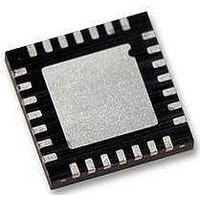
WM8986GECO/V Wolfson Microelectronics, WM8986GECO/V Datasheet - Page 54

WM8986GECO/V
Manufacturer Part Number
WM8986GECO/V
Description
Audio Amplifiers Class D Headphone DAC + Line Out
Manufacturer
Wolfson Microelectronics
Datasheet
1.WM8986GECOV.pdf
(88 pages)
Specifications of WM8986GECO/V
Product
Class-D
Output Power
40 mW
Thd Plus Noise
- 86 dB
Operating Supply Voltage
1.71 V to 3.6 V, 2.5 V to 3.6 V
Maximum Operating Temperature
+ 85 C
Mounting Style
SMD/SMT
Audio Load Resistance
16 Ohms
Minimum Operating Temperature
- 40 C
Output Signal Type
Differential
Supply Voltage (max)
3.6 V
Supply Voltage (min)
1.71 V, 2.5 V
Output Type
Differential
Package / Case
QFN-28
Lead Free Status / RoHS Status
Lead free / RoHS Compliant
WM8986
AUDIO SAMPLE RATES
w
Table 33 Clock Control
The CLKSEL bit selects the internal source of the Master clock from the PLL (CLKSEL=1) or from
MCLK (CLKSEL=0). When the internal clock is switched from one source to another using the
CLKSEL bit, the clock originally selected must generate at least one falling edge after CLKSEL has
changed for the switching of clocks to be successful.
EXAMPLE:
If the PLL is the current source of the internal clock (CLKSEL=1) and it is required to switch to the
MCLK, change CLKSEL to select MCLK (CLKSEL=0) and then disable PLL (PLLEN=0).
The WM8986 DAC limiter characteristics are sample rate dependent. SR should be set to the
correct sample rate or the closest value if the actual sample rate is not available.
If a sample rate that is not explicitly supported by the SR register settings is required then the closest
SR value to that sample rate should be chosen. The DAC limiter characteristics will scale
appropriately.
R6 (06h)
Clock
Generation
Control
REGISTER
REGISTER
ADDRESS
ADDRESS
0
4:2
7:5
8
BIT
BIT
MS
BCLKDIV
MCLKDIV
CLKSEL
LABEL
LABEL
DEFAULT
0
000
010
1
DEFAULT
Sets the chip to be master over LRC
and BCLK
0 = BCLK and LRC clock are inputs
1 = BCLK and LRC clock are outputs
generated by the WM8986 (MASTER)
Configures the BCLK output frequency,
for use when the chip is master over
BCLK.
000 = divide by 1 (BCLK=SYSCLK)
001 = divide by 2 (BCLK=SYSCLK/2)
010 = divide by 4 (BCLK=SYSCLK/4)
011 = divide by 8 (BCLK=SYSCLK/8)
100 = divide by 16 (BCLK=SYSCLK/16)
101 = divide by 32 (BCLK=SYSCLK/32)
110 = reserved
111 = reserved
Sets the scaling for SYSCLK clock
output (under control of CLKSEL)
000 = divide by 1 (LRC=SYSCLK/128)
001 = divide by 1.5 (LRC=SYSCLK/192)
010 = divide by 2 (LRC=SYSCLK/256)
011 = divide by 3 (LRC=SYSCLK/384)
100 = divide by 4 (LRC=SYSCLK/512)
101 = divide by 6 (LRC=SYSCLK/768)
110 = divide by 8 (LRC=SYSCLK/1024)
111 = divide by 12 (LRC=SYSCLK/1536)
Controls the source of the clock for all
internal operation:
0 = MCLK
1 = PLL output
DESCRIPTION
DESCRIPTION
PD, Rev 4.1, June 2009
Production Data
54


