TQP3M9009-PCB-IF TriQuint, TQP3M9009-PCB-IF Datasheet
TQP3M9009-PCB-IF
Specifications of TQP3M9009-PCB-IF


Related parts for TQP3M9009-PCB-IF


TQP3M9009-PCB-IF Summary of contents
Page 1
... High input power capability +5V Single Supply, 125 mA Current SOT-89 Package General Description The TQP3M9009 is a cascadable, high linearity gain block amplifier in a low-cost surface-mount package. At 1.9 GHz, the amplifier is targeted to provide 21.8 dB gain, +39.5 dBm OIP3, and 1.3 dB Noise Figure while only drawing 125 mA current ...
Page 2
... TQP3M9009 High Linearity LNA Gain Block Specifications Absolute Maximum Ratings Parameter Storage Temperature RF Input Power,CW,50 Ω 25ºC +23 dBm Device Voltage,V dd Reverse Device Voltage Thermal Resistance (junction to case) 34 Junction Temperature For 10 hours MTTF Operation of this device outside the parameter ranges given above may cause permanent damage. ...
Page 3
... TriQuint Semiconductor, Inc. Frequency (MHz) TQP3M9009-PCB_IF 50 - 500 TQP3M9009 1000 pF 0.01 uF 330 nH Do Not Place 0 Ω Frequency (MHz) 2000 2500 Disclaimer: Subject to change without - Connecting the Digital World to the Global Network +5Vdd TQP3M9009-PCB_RF 500 - 4000 100 pF 0. 3500 noticee ® ...
Page 4
... TQP3M9009 High Linearity LNA Gain Block Typical Performance 500-4000 MHz Test conditions unless otherwise noted: +25ºC, +5V, 125 mA, 50 Ω system. The data shown below is measured on TQP3M9009-PCB_RF. Frequency Gain Input Return Loss Output Return Loss Output P1dB OIP3 [1] Noise Figure [2] Notes: OIP3 measured with two tones at an output power of +3 dBm / tone separated by 1 MHz. The suppression on the largest IM3 product is 1 ...
Page 5
... TQP3M9009 High Linearity LNA Gain Block RF Performance Plots OIP3 vs. Pout / tone over Temp Freq = 1900 MHz, 1 MHz Spacing + + Pout / tone (dBm) OIP3 vs. Vdd F=1900 MHz, 1 MHz Spacing, T=+25⁰C, 3dBm / tone 3.25 3.5 3.75 4 4.25 4.5 Vdd (V) Idd vs. Vdd T=25⁰C, CW Signal ...
Page 6
... TQP3M9009 High Linearity LNA Gain Block Typical Performance 50-500 MHz Test conditions unless otherwise noted: +25ºC, +5V, 125 mA, 50 Ω system. The data shown below is measured on TQP3M9009-PCB_IF. Frequency Gain Input Return Loss Output Return Loss Output P1dB OIP3 [1] Noise Figure [2] Notes: OIP3 measured with two tones at an output power of +3 dBm / tone separated by 1 MHz. The suppression on the largest IM3 product is 1 ...
Page 7
... TQP3M9009 High Linearity LNA Gain Block IF Performance Plots OIP3 vs. Frequency over Temp 1 MHz Spacing, 3 dBm/tone -40 C + 100 200 300 Pout / tone (dBm) Advanced Data Sheet: Rev B 03/29/10 © 2009 TriQuint Semiconductor, Inc. P1dB vs. Frequency over Temp 100 400 500 - Connecting the Digital World to the Global Network ...
Page 8
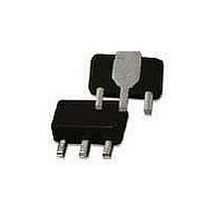
... TQP3M9009 High Linearity LNA Gain Block Pin Configuration and Description Pin Symbol GND 3 RFout / Vdd Applications Information PC Board Layout Top RF layer is .014” NELCO N4000-13, є layers (0.062” thick) for mechanical rigidity. layers are 1-oz copper. 50 ohm Microstrip line details: width = .029” ...
Page 9
... TQP3M9009 High Linearity LNA Gain Block Mechanical Information Package Information and Dimensions This package is lead-free/RoHS- compliant. The plating material on the leads is NiPdAu compatible with both lead-free (maximum 260 °C reflow temperature) and lead (maximum 245 °C reflow temperature) soldering processes. The component will be marked with a “ ...
Page 10
... TQP3M9009 High Linearity LNA Gain Block Product Compliance Information ESD Information ESD Rating: Class 1A Passes ≥ 250 V to < 500 V. Value: Test: Human Body Model (HBM) Standard: JEDEC Standard JESD22-A114 ESD Rating: Class IV Passes ≥ 1000 V Value: Test: Charged Device Model (CDM) ...