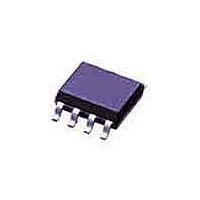
TISP8201MDR-S Bourns Inc., TISP8201MDR-S Datasheet - Page 8

TISP8201MDR-S
Manufacturer Part Number
TISP8201MDR-S
Description
Sidacs PROTECTOR - BUFFERED N-GATE PROG. PROT.
Manufacturer
Bourns Inc.
Datasheet
1.TISP8201MDR-S.pdf
(11 pages)
Specifications of TISP8201MDR-S
Breakover Current Ibo Max
11 A
Rated Repetitive Off-state Voltage Vdrm
120 V
Off-state Leakage Current @ Vdrm Idrm
0.005 mA
Mounting Style
SMD/SMT
Package / Case
SOIC-8
Lead Free Status / RoHS Status
Lead free / RoHS Compliant
Available stocks
Company
Part Number
Manufacturer
Quantity
Price
Part Number:
TISP8201MDR-S
Manufacturer:
BOURNS/伯恩斯
Quantity:
20 000
The negative protection voltage, V (BO) , will be the sum of the gate supply (V BATH ) and the TISP8200M peak gate(terminal)-cathode voltage
(V GT ). Under a.c. overvoltage conditions V GT will be less than 2.0 V. The integrated transistor buffer in the TISP8200M greatly reduces
protector’s source and sink current loading on the V BATH supply. Without the transistor, the SCR gate current would charge the V BATH supply.
An electronic power supply is not usually designed to be charged like a battery. As a result, the electronic supply would switch off and the SCR
gate current would provide the SLIC supply current. Normally the SLIC current would be less than the gate current, which would cause the
supply voltage to increase and destroy the SLIC by a supply overvoltage. Older designs using just SCRs needed to incorporate a sacrificial
zener diode across the supply line to go short if the supply voltage increased too much. The integrated transistor buffer removes the charging
problem and the need for a safety zener.
Fast rising impulses will cause short term overshoots in gate-cathode voltage. The negative protection voltage under impulse conditions will
also be increased if there is a long connection between the gate decoupling capacitor, C1, and the gate terminal. During the initial rise of a fast
impulse, the gate current (I G ) is the same as the cathode current (I K ). Rates of 60 A/µs can cause inductive voltages of 0.6 V in 2.5 cm of
printed wiring track. To minimize this inductive voltage increase of protection voltage, the length of the capacitor to gate terminal tracking
should be minimized.
The TISP8201M (buffered) gate is connected to the positive SLIC battery feed voltage (V BATR ) to provide the protection reference voltage.
Positive overvoltages are initially clipped close to the SLIC positive supply rail value (V BATR ) by the conduction of the TISP8201M transistor
base-emitter and the SCR gate-anode junctions. If sufficient current is available from the overvoltage, then the SCR will crowbar into a low
voltage ground referenced on-state condition. As the overvoltage subsides the SLIC pulls the conductor voltage down to its normal negative
value and this commutates the conducting SCR into a reverse biassed condition.
Figure 6 shows the protector electrodes. The package terminal designated gate, G, is the transistor base, B, electrode connection and so is
marked as B (G). The following junctions are subject to voltage stress: Transistor EB and CB, SCR AK (reverse and off state). This clause
covers the necessary testing to ensure the junctions are good.
Testing transistor EB and SCR AK reverse:
other protector. For the TISP8200M, the SCR has V BATR plus the TISP8201M overshoot above V BATR . The transistor EB has an additional
V BATH voltage applied (see Figure 7). The reverse current, I R , flowing into the K terminal will be the sum of the transistor I EB and the actual
internal SCR I R . The reverse voltage applied to the K terminal is the TISP8201M protection voltage, V (BO) (V BATR plus overshoot), and the G
terminal has V BATH . Similarly for the TISP8201M, I R is measured with the TISP8200M V (BO) applied and it is the sum of the transistor I EB and
the actual internal SCR I R . V BATR is applied to the G terminal.
MAY 1998 - REVISED JANUARY 2007
Specifications are subject to change without notice.
Customers should verify actual device performance in their specific applications.
Operation of Gated Protectors (Continued)
Voltage Stress Levels on the TISP8200M and TISP8201M
TISP8200M & TISP8201M
RING
TIP
AI8XAD
I
A
The highest reverse EB voltage and reverse AK voltage occurs during the overshoot period of the
Figure 5. Overvoltage Conditions
8201M
TISP
I
G
I
K
0 V
8200M
TISP
100 nF
V
C2
BATH
I
100 nF
G
C1
V
BATR
SLIC
0 V


