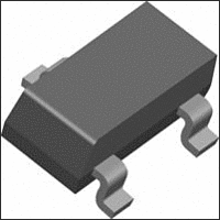
SST5485-E3 Vishay, SST5485-E3 Datasheet - Page 3

SST5485-E3
Manufacturer Part Number
SST5485-E3
Description
JFET 35V 4mA
Manufacturer
Vishay
Specifications of SST5485-E3
Configuration
Single
Transistor Polarity
N-Channel
Package / Case
TO-236
Gate-source Breakdown Voltage
- 25 V
Maximum Operating Temperature
+ 150 C
Maximum Drain Gate Voltage
- 25 V
Minimum Operating Temperature
- 55 C
Mounting Style
SMD/SMT
Breakdown Voltage Vbr
-25V
Gate-source Cutoff Voltage Vgs(off) Max
-4V
Power Dissipation Pd
350mW
Operating Temperature Range
-55°C To +150°C
No. Of Pins
3
Continuous Drain Current Id
10mA
Channel Type
N
Gate-source Voltage (max)
25V
Drain-gate Voltage (max)
-25V
Operating Temperature (min)
-55C
Operating Temperature (max)
150C
Operating Temperature Classification
Military
Mounting
Surface Mount
Pin Count
3
Lead Free Status / RoHS Status
Lead free / RoHS Compliant
Lead Free Status / RoHS Status
Lead free / RoHS Compliant, Lead free / RoHS Compliant
Notes
a.
b.
c.
d.
Stresses beyond those listed under “Absolute Maximum Ratings” may cause permanent damage to the device. These are stress ratings only, and functional operation
of the device at these or any other conditions beyond those indicated in the operational sections of the specifications is not implied. Exposure to absolute maximum
rating conditions for extended periods may affect device reliability.
S-50148—Rev. G, 24-Jan-05
Document Number: 70246
SPECIFICATIONS FOR SST SERIES (T
Static
Gate-Source
Breakdown Voltage
Gate-Source Cutoff Voltage
Saturation Drain Current
Gate Reverse Current
Gate Reverse Current
Gate Operating Current
Gate-Source
Forward Voltage
Dynamic
Common-Source
Forward Transconductance
Common-Source
Output Conductance
Common-Source
Input Capacitance
Common-Source
Reverse Transfer
Capacitance
Common-Source
Output Capacitance
Equivalent Input
Noise Voltage
High-Frequency
Common-Source
Common-Source
Transconductance
Common-Source
Common-Source
Output Conductance
Common-Source
Common-Source
Input Conductance
Common-Source
Common-Source
Power Gain
Noise Figure
Typical values are for DESIGN AID ONLY, not guaranteed nor subject to production testing.
Pulse test: PW v300 ms duty cycle v3%.
This parameter not registered with JEDEC.
Not a production test.
g
Parameter
c
c
NO TAG
c
b
NO TAG
Symbol
V
V
V
(BR)GSS
I
I
C
GS(off)
I
C
C
G
G
GS(F)
Y
Y
DSS
GSS
GSS
g
Y
Y
NF
g
Y
Y
e
I
oss
G
os
rss
iss
os
fs
f
fs
i
is
ps
n
V
V
V
V
V
R
V
I
I
I
DS
DS
DS
DS
D
DS
D
D
GS
G
= 4 mA
= 4 mA
= 4 mA
R
V
= 1 kW
I
V
V
V
V
V
V
I
V
V
V
V
= 15 V
= 15 V
= 15 V
= 15 V
= 15 V
Test Conditions
G
R
G
= 0 V
GS
G
DS
DS
DS
DS
DS
DS
DS
DG
DS
DS
G
= 10 mA , V
= −1 mA , V
= 1 kW , f = 100 MHz
= −20 V, V
= 15 V, V
= 15 V, V
= 15 V, V
= 1 MW , f = 1 kHz
= 15 V, I
= 15 V, I
= 15 V, I
= 15 V, V
= 15 V, V
= 15 V, V
= 10 V, I
f = 100 MHz
A
f = 100 Hz
f = 1 MHz
f = 1 kHz
= 25_C UNLESS OTHERWISE NOTED)
D
D
D
D
DS
GS
GS
GS
GS
GS
GS
DS
= 10 nA
DS
=
= 1 mA
= 1 mA
f = 100 MHz
f = 400 MHz
f = 100 MHz
f = 400 MHz
f = 100 MHz
f = 400 MHz
f = 100 MHz
f = 400 MHz
f = 100 MHz
f = 400 MHz
T
1 mA
= 0 V
A
= 0 V
= 0 V
= 0 V
= 0 V
= 0 V
= 0 V
= 0 V
= 0 V
= 100_C
−0.002
Typ
−0.2
0.05
−35
−20
0.8
2.2
0.7
5.5
5.5
0.8
0.3
2.5
10
45
65
20
21
13
1
2
1
b
Min
−0.3
−25
1
3
SST5484
Max
−200
−3
−1
50
5
6
2N/SST5484 Series
Min
−0.5
−25
3.5
4
SST5485
Limits
Vishay Siliconix
Max
−200
−4
10
−1
60
7
Min
−25
−2
8
4
SST5486
www.vishay.com
Max Unit
−200
−6
20
−1
75
8
√Hz
mA
mS
mS
mS
mS
mS
nV⁄
nA
nA
pA
mS
pF
mS
mS
dB
V
V
V
NH
3


