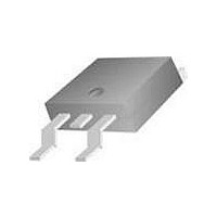
FDD86102 Fairchild Semiconductor, FDD86102 Datasheet - Page 2

FDD86102
Manufacturer Part Number
FDD86102
Description
MOSFET Power 100V N-Channel PowerTrench
Manufacturer
Fairchild Semiconductor
Datasheet
1.FDD86102.pdf
(6 pages)
Specifications of FDD86102
Gate Charge Qg
13.4 nC
Minimum Operating Temperature
- 55 C
Transistor Polarity
N-Channel
Resistance Drain-source Rds (on)
19 mOhms
Forward Transconductance Gfs (max / Min)
21 S
Drain-source Breakdown Voltage
100 V
Gate-source Breakdown Voltage
20 V
Continuous Drain Current
8 A
Power Dissipation
3.1 W
Maximum Operating Temperature
+ 125 C
Mounting Style
SMD/SMT
Package / Case
DPAK
Lead Free Status / RoHS Status
Lead free / RoHS Compliant
Available stocks
Company
Part Number
Manufacturer
Quantity
Price
Company:
Part Number:
FDD86102
Manufacturer:
FSC
Quantity:
20 000
Part Number:
FDD86102
Manufacturer:
FCS
Quantity:
20 000
Part Number:
FDD86102LZ
Manufacturer:
FAIRCHILD/ن»™ç«¥
Quantity:
20 000
FDD86102 Rev.C2
Electrical Characteristics
Off Characteristics
On Characteristics
Dynamic Characteristics
Switching Characteristics
Drain-Source Diode Characteristics
Notes:
1. R
3. Starting T
BV
∆BV
I
I
V
r
g
C
C
C
R
t
t
t
t
Q
Q
Q
Q
V
t
Q
2. Pulse Test: Pulse Width < 300 µs, Duty cycle < 2.0%.
∆V
DSS
GSS
d(on)
r
d(off)
f
rr
DS(on)
FS
GS(th)
SD
R
iss
oss
rss
g
∆T
∆T
g
g
gs
gd
rr
Symbol
θJA
θJC
DSS
GS(th)
DSS
J
J
is the sum of the junction-to-case and case-to-ambient thermal resistance where the case thermal reference is defined as the solder mounting surface of the drain pins.
is guaranteed by design while R
J
= 25
°
Drain to Source Breakdown Voltage
Breakdown Voltage Temperature
Coefficient
Zero Gate Voltage Drain Current
Gate to Source Leakage Current
Gate to Source Threshold Voltage
Gate to Source Threshold Voltage
Temperature Coefficient
Static Drain to Source On Resistance
Forward Transconductance
Input Capacitance
Output Capacitance
Reverse Transfer Capacitance
Gate Resistance
Turn-On Delay Time
Rise Time
Turn-Off Delay Time
Fall Time
Total Gate Charge
Total Gate Charge
Gate to Source Gate Charge
Gate to Drain “Miller” Charge
Source to Drain Diode Forward Voltage
Reverse Recovery Time
Reverse Recovery Charge
C, L = 3 mH, I
AS
(Note 2)
= 9 A, V
θJA
Parameter
is determined by the user’s board design.
DD
= 100 V, V
T
J
a. 40 °C/W when mounted on a
GS
= 25 °C unless otherwise noted
1 in
= 10 V.
2
pad of 2 oz copper.
V
V
V
V
V
f = 1 MHz
V
I
V
V
V
V
V
V
I
I
I
V
V
D
F
D
D
DD
GS
GS
GS
GS
GS
GS
GS
DS
DS
GS
GS
DS
GS
= 8 A, di/dt = 100 A/µs
= 250 µA, referenced to 25 °C
= 250 µA, V
= 250 µA, referenced to 25 °C
= 50 V, V
= 50 V, I
= 10 V, R
= 0 V to 10 V
= 0 V to 5 V
= 10 V, I
= 0 V, I
= 0 V, I
= 80 V, V
= V
= 10 V, I
= 6 V, I
= 10 V, I
= ±20 V, V
2
DS
Test Conditions
, I
D
S
S
D
D
D
D
D
= 8 A
= 2.6 A
= 6 A
GS
GEN
GS
= 250 µA
GS
= 8 A,
= 8 A
= 8 A, T
= 8 A
DS
= 0 V,
= 0 V
= 0 V
= 0 V
= 6 Ω
V
I
D
DD
= 8 A
J
= 50 V,
= 125 °C
(Note 2)
(Note 2)
b. 96 °C/W when mounted on a
Min
100
minimum pad of 2 oz copper.
2
13.4
13.4
-8.5
780
180
0.8
0.7
0.4
Typ
3.1
15
7.6
3.0
2.9
7.6
4.0
3.7
43
43
19
26
33
21
67
1035
±100
Max
240
1.3
1.2
25
68
68
24
38
44
15
10
24
10
19
11
www.fairchildsemi.com
4
1
mV/°C
mV/°C
Units
mΩ
nC
pF
pF
pF
µA
nA
nC
nC
nC
nC
ns
Ω
ns
ns
ns
ns
V
V
S
V


