SiHF16N50C-E3 Vishay, SiHF16N50C-E3 Datasheet - Page 7
SiHF16N50C-E3
Manufacturer Part Number
SiHF16N50C-E3
Description
MOSFET Power N-Channel 500V
Manufacturer
Vishay
Datasheet
1.SIHP16N50C-E3.pdf
(8 pages)
Specifications of SiHF16N50C-E3
Transistor Polarity
N-Channel
Gate Charge Qg
68 nC
Minimum Operating Temperature
- 55 C
Configuration
Single
Forward Transconductance Gfs (max / Min)
3 S
Drain-source Breakdown Voltage
500 V
Continuous Drain Current
16 A
Power Dissipation
38 W
Maximum Operating Temperature
+ 150 C
Mounting Style
Through Hole
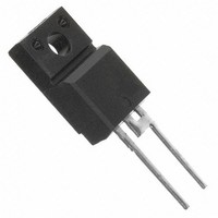
Package / Case
TO-220
Drain Source Voltage Vds
500V
On Resistance Rds(on)
0.31ohm
Rds(on) Test Voltage Vgs
10V
Voltage Vgs Max
30V
Operating Temperature Range
-55°C To +150°C
Lead Free Status / RoHS Status
Lead free / RoHS Compliant
Lead Free Status / RoHS Status
Lead free / RoHS Compliant, Lead free / RoHS Compliant
Available stocks
Company
Part Number
Manufacturer
Quantity
Price


Vishay Siliconix maintains worldwide manufacturing capability. Products may be manufactured at one of several qualified locations. Reliability data for Silicon
Technology and Package Reliability represent a composite of all qualified locations. For related documents such as package/tape drawings, part marking, and
reliability data, see www.vishay.com/ppg?91401.
Document Number: 91401
S10-0811-Rev. A, 12-Apr-10
Re-applied
voltage
Reverse
recovery
current
+
-
R
D.U.T.
G
*
Driver gate drive
D.U.T. I
D.U.T. V
Inductor current
V
GS
= 5 V for logic level devices
P.W.
SD
DS
waveform
waveform
SiHP16N50C, SiHB16N50C, SiHF16N50C
Fig. 15 - For N-Channel
Peak Diode Recovery dV/dt Test Circuit
Ripple ≤ 5 %
Body diode
Period
Body diode forward
+
-
• dV/dt controlled by R
• Driver same type as D.U.T.
• I
• D.U.T. - device under test
SD
Diode recovery
current
controlled by duty factor "D"
Circuit layout considerations
dV/dt
forward drop
• Low stray inductance
• Ground plane
• Low leakage inductance
dI/dt
current transformer
D =
-
G
Period
P.W.
+
V
V
I
SD
GS
DD
= 10 V*
+
-
V
DD
Vishay Siliconix
www.vishay.com
7
Related parts for SiHF16N50C-E3
Image
Part Number
Description
Manufacturer
Datasheet
Request
R

Part Number:
Description:
357-036-542-201 CARDEDGE 36POS DL .156 BLK LOPRO
Manufacturer:
Vishay
Datasheet:
Part Number:
Description:
357-036-542-201 CARDEDGE 36POS DL .156 BLK LOPRO
Manufacturer:
Vishay
Datasheet:
Part Number:
Description:
357-036-542-201 CARDEDGE 36POS DL .156 BLK LOPRO
Manufacturer:
Vishay
Datasheet:
Part Number:
Description:
357-036-542-201 CARDEDGE 36POS DL .156 BLK LOPRO
Manufacturer:
Vishay
Datasheet:
Part Number:
Description:
357-036-542-201 CARDEDGE 36POS DL .156 BLK LOPRO
Manufacturer:
Vishay
Datasheet:
Part Number:
Description:
357-036-542-201 CARDEDGE 36POS DL .156 BLK LOPRO
Manufacturer:
Vishay
Datasheet:
Part Number:
Description:
357-036-542-201 CARDEDGE 36POS DL .156 BLK LOPRO
Manufacturer:
Vishay
Datasheet:
Part Number:
Description:
357-036-542-201 CARDEDGE 36POS DL .156 BLK LOPRO
Manufacturer:
Vishay
Datasheet:
Part Number:
Description:
357-036-542-201 CARDEDGE 36POS DL .156 BLK LOPRO
Manufacturer:
Vishay
Datasheet:
Part Number:
Description:
357-036-542-201 CARDEDGE 36POS DL .156 BLK LOPRO
Manufacturer:
Vishay
Datasheet:
Part Number:
Description:
357-036-542-201 CARDEDGE 36POS DL .156 BLK LOPRO
Manufacturer:
Vishay
Datasheet:
Part Number:
Description:
357-036-542-201 CARDEDGE 36POS DL .156 BLK LOPRO
Manufacturer:
Vishay
Datasheet:
Part Number:
Description:
357-036-542-201 CARDEDGE 36POS DL .156 BLK LOPRO
Manufacturer:
Vishay
Datasheet:
Part Number:
Description:
357-036-542-201 CARDEDGE 36POS DL .156 BLK LOPRO
Manufacturer:
Vishay
Datasheet:
Part Number:
Description:
357-036-542-201 CARDEDGE 36POS DL .156 BLK LOPRO
Manufacturer:
Vishay
Datasheet: