2N6661-E3 Vishay, 2N6661-E3 Datasheet - Page 2
2N6661-E3
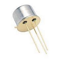
Manufacturer Part Number
2N6661-E3
Description
MOSFET Power 90V 0.9A
Manufacturer
Vishay
Datasheet
1.2N6661-E3.pdf
(6 pages)
Specifications of 2N6661-E3
Transistor Polarity
N-Channel
Package / Case
TO-205AD
Drain-source Breakdown Voltage
90 V
Minimum Operating Temperature
- 55 C
Configuration
Single
Resistance Drain-source Rds (on)
4 Ohm @ 10 V
Gate-source Breakdown Voltage
+/- 20 V
Continuous Drain Current
0.9 A
Power Dissipation
6250 mW
Maximum Operating Temperature
+ 150 C
Mounting Style
Stud
On Resistance Rds(on)
4ohm
Current Rating
900mA
Leaded Process Compatible
Yes
Gate-source Voltage
2V
Mounting Type
Through Hole
Lead Free Status / RoHS Status
Lead free / RoHS Compliant
Lead Free Status / RoHS Status
Lead free / RoHS Compliant, Lead free / RoHS Compliant


2N6661-2
Vishay Siliconix
Notes:
a. For DESIGN AID ONLY, not subject to production testing.
b. Pulse test; pulse width ≤ 300 µs, duty cycle ≤ 2 %.
c. Switching time is essentially independent of operating temperature.
d. This parameter not registered with JEDEC.
Stresses beyond those listed under “Absolute Maximum Ratings” may cause permanent damage to the device. These are stress ratings only, and functional operation
of the device at these or any other conditions beyond those indicated in the operational sections of the specifications is not implied. Exposure to absolute maximum
rating conditions for extended periods may affect device reliability.
www.vishay.com
2
Zero Gate Voltage Drain Current
SPECIFICATIONS T
Parameter
Static
Drain-Source Breakdown Voltage
Gate-Threshold Voltage
Gate-Body Leakage
On-State Drain Current
Drain-Source On-Resistance
Forward Transconductance
Diode Forward Voltage
Dynamic
Input Capacitance
Output Capacitance
Reverse Transfer Capacitance
Drain-Source Capacitance
Switching
Turn-On Time
Turn-Off Time
c
b
b
b
J
= 25 °C, unless otherwise noted
Symbol
R
V
I
I
C
DS(on)
t
V
GS(th)
I
D(on)
V
C
C
C
GSS
t
DSS
OFF
g
ON
DS
SD
oss
rss
iss
fs
ds
New Product
V
V
V
V
DS
V
V
I
I
DS
V
V
V
DS
V
S
D
DS
V
DS
DS
DD
GS
DS
GS
Test Conditions
GS
= 0.86 A, V
= 25 V, V
= 7.5 V, I
≅ 1 A, V
= 0 V, V
= 10 V, V
= 72 V, V
= 72 V, V
= V
= 25 V,
= 0 V, I
T
R
= 5 V, I
= 10 V, I
A
f = 1 MHz
GS
GS
= 125 °C
= 23 Ω
, I
GEN
GS
D
D
RL
D
GS
D
GS
GS
GS
GS
= 10 µA
= 0.475 A
D
= 0.3 A
= 1 mA
= ± 20 V
T
= 23 Ω
= 10 V
= 1 A
T
T
T
= 10 V
A
= 0 V
= 0 V
= 0 V
= 0 V,
A
A
A
= 125 °C
= - 55 °C
= 125 °C
= 125 °C
d
Typ.
125
340
1.6
1.8
1.3
1.8
3.8
3.6
6.7
0.9
35
15
30
2
6
8
a
Min.
170
0.8
0.3
0.7
90
S-81302-Rev. A, 09-Jun-08
Document Number: 68632
Limits
± 100
± 500
Max.
100
2.5
5.3
7.5
1.4
50
40
10
10
10
2
1
4
Unit
mS
nA
µA
pF
ns
Ω
V
A
V
Related parts for 2N6661-E3
Image
Part Number
Description
Manufacturer
Datasheet
Request
R

Part Number:
Description:
N CH MOSFET, 90V, 900mA, TO-205AD
Manufacturer:
Vishay
Datasheet:

Part Number:
Description:
357-036-542-201 CARDEDGE 36POS DL .156 BLK LOPRO
Manufacturer:
Vishay
Datasheet:
Part Number:
Description:
357-036-542-201 CARDEDGE 36POS DL .156 BLK LOPRO
Manufacturer:
Vishay
Datasheet:
Part Number:
Description:
357-036-542-201 CARDEDGE 36POS DL .156 BLK LOPRO
Manufacturer:
Vishay
Datasheet:
Part Number:
Description:
357-036-542-201 CARDEDGE 36POS DL .156 BLK LOPRO
Manufacturer:
Vishay
Datasheet:
Part Number:
Description:
357-036-542-201 CARDEDGE 36POS DL .156 BLK LOPRO
Manufacturer:
Vishay
Datasheet:
Part Number:
Description:
357-036-542-201 CARDEDGE 36POS DL .156 BLK LOPRO
Manufacturer:
Vishay
Datasheet:
Part Number:
Description:
357-036-542-201 CARDEDGE 36POS DL .156 BLK LOPRO
Manufacturer:
Vishay
Datasheet:
Part Number:
Description:
357-036-542-201 CARDEDGE 36POS DL .156 BLK LOPRO
Manufacturer:
Vishay
Datasheet:
Part Number:
Description:
357-036-542-201 CARDEDGE 36POS DL .156 BLK LOPRO
Manufacturer:
Vishay
Datasheet:
Part Number:
Description:
357-036-542-201 CARDEDGE 36POS DL .156 BLK LOPRO
Manufacturer:
Vishay
Datasheet:
Part Number:
Description:
357-036-542-201 CARDEDGE 36POS DL .156 BLK LOPRO
Manufacturer:
Vishay
Datasheet:
Part Number:
Description:
357-036-542-201 CARDEDGE 36POS DL .156 BLK LOPRO
Manufacturer:
Vishay
Datasheet:
Part Number:
Description:
357-036-542-201 CARDEDGE 36POS DL .156 BLK LOPRO
Manufacturer:
Vishay
Datasheet: