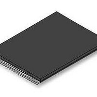
S29GL512P11TFI010 Spansion Inc., S29GL512P11TFI010 Datasheet - Page 11

S29GL512P11TFI010
Manufacturer Part Number
S29GL512P11TFI010
Description
Flash 3V 512Mb Mirrorbit highest address110ns
Manufacturer
Spansion Inc.
Specifications of S29GL512P11TFI010
Memory Type
NOR
Memory Size
512 Mbit
Access Time
110 ns
Data Bus Width
8 bit, 16 bit
Architecture
Uniform
Interface Type
Page-mode
Supply Voltage (max)
3.6 V
Supply Voltage (min)
2.7 V
Maximum Operating Current
50 mA
Mounting Style
SMD/SMT
Operating Temperature
+ 85 C
Package / Case
TSOP-56
Memory Configuration
128K X 16
Ic Interface Type
Parallel
Supply Voltage Range
2.7V To 3.6V
Memory Case Style
TSOP
No. Of Pins
56
Cell Type
NOR
Density
512Mb
Access Time (max)
110ns
Boot Type
Not Required
Address Bus
26/25Bit
Operating Supply Voltage (typ)
3/3.3V
Operating Temp Range
-40C to 85C
Package Type
TSOP
Sync/async
Asynchronous
Operating Temperature Classification
Industrial
Operating Supply Voltage (min)
2.7V
Operating Supply Voltage (max)
3.6V
Word Size
8/16Bit
Number Of Words
64M/32M
Supply Current
110mA
Mounting
Surface Mount
Pin Count
56
Lead Free Status / RoHS Status
Lead free / RoHS Compliant
Lead Free Status / RoHS Status
Lead free / RoHS Compliant, Lead free / RoHS Compliant
Available stocks
Company
Part Number
Manufacturer
Quantity
Price
Company:
Part Number:
S29GL512P11TFI010
Manufacturer:
SPANSION
Quantity:
65
Company:
Part Number:
S29GL512P11TFI010
Manufacturer:
SPANSION
Quantity:
4 000
Part Number:
S29GL512P11TFI010
Manufacturer:
SPANSION
Quantity:
20 000
Company:
Part Number:
S29GL512P11TFI010D
Manufacturer:
SPANSION
Quantity:
7 358
2. Input/Output Descriptions & Logic Symbol
November 28, 2007 S29GL-P_00_A8
Table 2.1
DQ14–DQ0
WP#/ACC
DQ15/A-1
RESET#
Symbol
A25–A0
RY/BY#
BYTE#
WE#
OE#
RFU
CE#
V
V
V
NC
CC
SS
IO
identifies the input and output package connections provided on the device.
D a t a
No Connect
Reserved
Supply
Supply
Supply
Output
Type
Input
Input
Input
Input
Input
Input
Input
I/O
I/O
S h e e t
Address lines for GL01GP
A24–A0 for GL512P
A23–A0 for GL256P,
A22–A0 for GL128P.
Data input/output.
DQ15: Data input/output in word mode.
A-1: LSB address input in byte mode.
Chip Enable.
Output Enable.
Write Enable.
Device Power Supply.
Versatile IO Input.
Ground.
Not connected internally.
Ready/Busy. Indicates whether an Embedded Algorithm is in progress or complete. At
V
Selects data bus width. At VIL, the device is in byte configuration and data I/O pins DQ0-
DQ7 are active and DQ15/A-1 becomes the LSB address input. At VIH, the device is in
word configuration and data I/O pins DQ0-DQ15 are active.
Hardware Reset. Low = device resets and returns to reading array data.
Write Protect/Acceleration Input. At V
outermost sectors. At V
unlock bypass mode. Should be at V
up; when unconnected, WP# is at V
Reserved for future use.
S29GL-P MirrorBit
IL
, the device is actively erasing or programming. At High Z, the device is in ready.
( P r e l i m i n a r y )
Table 2.1 Input/Output Descriptions
®
Flash Family
HH
, accelerates programming; automatically places device in
IH
IH
IL
.
Description
, disables program and erase functions in the
for all other conditions. WP# has an internal pull-
11


