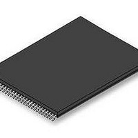
S29GL512P11TFI010 Spansion Inc., S29GL512P11TFI010 Datasheet - Page 60

S29GL512P11TFI010
Manufacturer Part Number
S29GL512P11TFI010
Description
Flash 3V 512Mb Mirrorbit highest address110ns
Manufacturer
Spansion Inc.
Specifications of S29GL512P11TFI010
Memory Type
NOR
Memory Size
512 Mbit
Access Time
110 ns
Data Bus Width
8 bit, 16 bit
Architecture
Uniform
Interface Type
Page-mode
Supply Voltage (max)
3.6 V
Supply Voltage (min)
2.7 V
Maximum Operating Current
50 mA
Mounting Style
SMD/SMT
Operating Temperature
+ 85 C
Package / Case
TSOP-56
Memory Configuration
128K X 16
Ic Interface Type
Parallel
Supply Voltage Range
2.7V To 3.6V
Memory Case Style
TSOP
No. Of Pins
56
Cell Type
NOR
Density
512Mb
Access Time (max)
110ns
Boot Type
Not Required
Address Bus
26/25Bit
Operating Supply Voltage (typ)
3/3.3V
Operating Temp Range
-40C to 85C
Package Type
TSOP
Sync/async
Asynchronous
Operating Temperature Classification
Industrial
Operating Supply Voltage (min)
2.7V
Operating Supply Voltage (max)
3.6V
Word Size
8/16Bit
Number Of Words
64M/32M
Supply Current
110mA
Mounting
Surface Mount
Pin Count
56
Lead Free Status / RoHS Status
Lead free / RoHS Compliant
Lead Free Status / RoHS Status
Lead free / RoHS Compliant, Lead free / RoHS Compliant
Available stocks
Company
Part Number
Manufacturer
Quantity
Price
Company:
Part Number:
S29GL512P11TFI010
Manufacturer:
SPANSION
Quantity:
65
Company:
Part Number:
S29GL512P11TFI010
Manufacturer:
SPANSION
Quantity:
4 000
Part Number:
S29GL512P11TFI010
Manufacturer:
SPANSION
Quantity:
20 000
Company:
Part Number:
S29GL512P11TFI010D
Manufacturer:
SPANSION
Quantity:
7 358
Notes
1. PA = program address, PD = program data, D
2. Illustration shows device in word mode.
Notes
1. Not 100% tested.
2. CE#, OE# = V
3. OE# = V
4. See
60
Addresses
Figure 11.3
RY/BY#
IL
ACC
WE#
Data
OE#
CE#
V
IL
CC
and
V
V
IL
Table 11.1
HH
or V
t
VCS
IH
for test specifications.
t
Program Command Sequence (last two cycles)
VHH
555h
t
CS
t
WC
Figure 11.10 Accelerated Program Timing Diagram
OUT
t
WP
t
is the true data at the program address.
DS
Figure 11.9 Program Operation Timings
A0h
t
DH
S29GL-P MirrorBit
t
CH
D a t a
t
WPH
t
AS
PA
S h e e t
t
AH
®
PD
Flash Family
t
BUSY
( P r e l i m i n a r y )
t
WHWH1
Read Status Data (last two cycles)
S29GL-P_00_A8 November 28, 2007
PA
Status
t
VHH
V
D
IL
OUT
PA
or V
t
RB
IH


