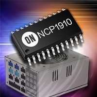
NCP1910A65DWR2G ON Semiconductor, NCP1910A65DWR2G Datasheet - Page 10

NCP1910A65DWR2G
Manufacturer Part Number
NCP1910A65DWR2G
Description
AC/DC Switching Converters GREENM COMBO 2GND N/SKIP
Manufacturer
ON Semiconductor
Type
Combo Controllerr
Datasheet
1.NCP1910A65DWR2G.pdf
(37 pages)
Specifications of NCP1910A65DWR2G
Input / Supply Voltage (max)
20 V
Switching Frequency
500 KHz
Operating Temperature Range
- 60 C to + 150 C
Mounting Style
SMD/SMT
Package / Case
SO-24
Maximum Operating Temperature
+ 150 C
Minimum Operating Temperature
- 60 C
Number Of Outputs
2
Output Current
5 mA
Lead Free Status / RoHS Status
Lead free / RoHS Compliant
Available stocks
Company
Part Number
Manufacturer
Quantity
Price
Company:
Part Number:
NCP1910A65DWR2G
Manufacturer:
ON Semiconductor
Quantity:
1 000
ELECTRICAL CHARACTERISTICS
= 12 V unless otherwise noted)
POWER FACTOR CORRECTION
LLC CONTROL SECTION
3. In normal operation, when the power supply is un−plugged, the bulk voltage goes down. At a first crossed level, the PG pin opens. Later,
4. Guaranteed by design.
V
V
LINE BROWN−OUT DETECTION
CURRENT MODULATION
OVER−VOLTAGE PROTECTION
UNDER−VOLTAGE PROTECTION
PFC ABNORMAL
OSCILLATOR
UVP(on)
UVP(off)
t
t
t
LBO(Pdblank)
PFCabnormal
LBO(Pdlimit)
V
when the bulk crosses a second level, the LLC turns off. There is no timing link between these events, except the bulk capacitor discharge
slope. However, if for an unknown reason the PFC is disabled (fault, short−circuit), the PG pin immediately opens and if sufficient voltage
is still present on the bulk (e.g. in high line condition), the LLC will be disabled after a typical time of 5 ms.
V
t
F
Symbol
F
V
DELOVP2
V
t
I
K
SS
skip,hyste
V
V
LBO(PD)
PFCflag
t
b,OVP2
Lsw,max
Lsw,min
V
V
OVP1H
UVP(H)
F
OVP1
t
DC
R
OVPH
I
I
OVP1
OVP2
UVP
refRt
M1
M2
Lsw
Skip
SS
RST
/V
/V
L
PREF
PREF
Pull Down V
Pull Down V
Time Delay to Confirm that V
Pull Down V
Multiplier Output Current (V
I
Multiplier Output Current (V
I
Internal Auto Recovery Over Voltage Threshold
Hysteresis of Internal Auto Recovery Over Voltage Threshold
(Note 4)
Propagation Delay (V
External Latched Over Voltage Threshold
The difference between V
V
External Latched OVP Integrating Filter Time Constant
Input bias current, OVP2
UVP Activate Threshold Ratio
UVP Deactivate Threshold Ratio
UVP Lockout Hysteresis
Propagation Delay (V
PFC Abnormal Delay Time (V
V
Minimum switching frequency, Rt = 70 kW on R
switching frequency, DT
Maximum switching frequency, DT
Operating Duty−Cycle symmetry
Reference voltage for oscillator charging current generation
Discharge switch resistance
Soft−start reset voltage
Skip cycle threshold, B version only
Hysteresis level on skip cycle comparator, B version only
CS
CS
OVP1
CTRL(min)
= 50 mA)
= 150 mA)
)/V
PREF
– 0.1 V)
LBO
LBO
LBO
)
Threshold
Time Limitation
Blanking Time
FB
FB
(For typical values T
L
= 108% V
< 8 % V
OVP2
= 300 ns, Rt = 7 kW on R
CTRL
CTRL
CTRL
CTRL
Rating
and V
PREF
=V
=V
is the maximum to Pull down V
PREF
L
= V
CTRL(max)
CTRL(max)
= 300 ns, Rt = 3.5 kW on R
OVP1
) to Drive Low
CTRL(max)
) to Drive Low
http://onsemi.com
over V
J
= 25°C, for min/max values T
– 0.2 V , V
– 0.2 V , V
t
pin
or V
PREF
10
t
pin
CTRL
((V
LBO
LBO
OVP2
=
= 3.6 V,
= 1.2 V,
t
−
pin
LBO
9 − 18
23, 20
9, 18
Pin
12
16
16
11
11
J
−
−
−
9
9
8
−
−
8
9
9
9
−
2
2
2
2
1
1
= −40°C to +125°C, Max T
2.536
2.595
24.25
3.33
Min
208
424
350
1.8
4.5
2.5
55
46
15
48
−
−
−
−
−
4
6
−
−
1
−
−
−
2.615
2.675
Typ
500
245
500
200
400
1.5
3.5
77
58
19
44
20
10
12
25
50
70
50
2
5
5
2
8
4
7
J
2.694
2.755
25.75
= 150°C, V
Max
24.5
3.67
282
575
450
2.2
6.1
7.5
2.1
90
72
60
12
18
52
−
−
−
−
−
−
−
−
−
Unit
kHz
kHz
kHz
sec
mV
mV
mV
mV
ms
ms
ms
mA
nA
ns
ms
ms
CC
%
%
%
%
%
V
V
V
V
W


