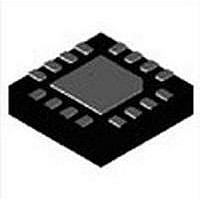
MAX5974AETE+ Maxim Integrated Products, MAX5974AETE+ Datasheet - Page 15

MAX5974AETE+
Manufacturer Part Number
MAX5974AETE+
Description
Current Mode PWM Controllers ACTIVE-CLAMPED CUR MODE PWM CONTLR
Manufacturer
Maxim Integrated Products
Datasheet
1.MAX5974DETE.pdf
(26 pages)
Specifications of MAX5974AETE+
Duty Cycle (max)
82 %
Mounting Style
SMD/SMT
Switching Frequency
600 KHz
Operating Supply Voltage
12 V to 21 V
Supply Current
1.8 mA
Maximum Operating Temperature
+ 85 C
Fall Time
14 ns
Minimum Operating Temperature
- 40 C
Rise Time
27 ns
Package / Case
TQFN-16
Lead Free Status / RoHS Status
Lead free / RoHS Compliant
The MAX5974A/MAX5974B/MAX5974C/MAX5974D are
optimized for controlling a 25W to 50W active-clamped,
self-driven synchronous rectification forward converter
in continuous-conduction mode. The main switch gate
driver (NDRV) and the active-clamped switch driver
(AUXDRV) are sized to optimize efficiency for 25W
design. The features-rich devices are ideal for PoE IEEE
802.3af/at-powered devices.
The MAX5974A/MAX5974C offer a 20V bootstrap UVLO
wake-up level with a 13V wide hysteresis. The low
startup and operating currents allow the use of a smaller
storage capacitor at the input without compromising
startup and hold times. The MAX5974A/MAX5974C are
well-suited for universal input (rectified 85V AC to 265V
AC) or telecom (-36V DC to -72V DC) power supplies.
The MAX5974B/MAX5974D have a UVLO rising threshold
of 10V and can accommodate for low-input voltage (12V
DC to 24V DC) power sources such as wall adapters.
Power supplies designed with the MAX5974A/MAX5974C
use a high-value startup resistor, R
reservoir capacitor, C
Circuits). During this initial period, while the voltage is
less than the internal bootstrap UVLO threshold, the
device typically consumes only 100FA of quiescent cur-
rent. This low startup current and the large bootstrap
UVLO hysteresis help to minimize the power dissipation
across R
voltage (265V AC).
Feed-forward maximum duty-cycle clamping detects chang-
es in line conditions and adjusts the maximum duty cycle
accordingly to eliminate the clamp voltage’s (i.e., the main
power FET’s drain voltage) dependence on the input voltage.
For EMI-sensitive applications, the programmable fre-
quency dithering feature allows up to Q10% variation in
the switching frequency. This spread-spectrum modula-
tion technique spreads the energy of switching harmon-
ics over a wider band while reducing their peaks, help-
ing to meet stringent EMI goals.
The devices include a cycle-by-cycle current limit
that turns off the main and AUX drivers whenever the
internally set threshold of 400mV is exceeded. Eight
consecutive occurrences of current-limit events trigger
hiccup mode, which protects external components by
halting switching for a period of time (t
ing the overload current to dissipate in the load and
body diode of the synchronous rectifier before soft-start
is reattempted.
IN
even at the high end of the universal AC input
Detailed Description
IN
(see the Typical Application
Active-Clamped, Spread-Spectrum,
IN
RSTRT
, that charges a
Current-Mode PWM Controllers
) and allow-
The reverse current-limit feature of the devices turns
the AUX driver off for the remaining off period when
V
transformer core from saturation due to excess reverse
current under some extreme transient conditions.
The advantages of current-mode control over voltage-
mode control are twofold. First, there is the feed-forward
characteristic brought on by the controller’s ability to adjust
for variations in the input voltage on a cycle-by-cycle basis.
Second, the stability requirements of the current-mode
controller are reduced to that of a single-pole system,
unlike the double pole in voltage-mode control.
The devices use a current-mode control loop where the
scaled output of the error amplifier (COMP) is compared
to a slope-compensated current-sense signal at CSSC.
The enable input EN is used to enable or disable the
device. Connect EN to IN for always enabled applica-
tions. Connecting EN to ground disables the device and
reduces current consumption to 150FA.
The enable input has an accurate threshold of 1.26V
(max). For applications that require a UVLO on the
power source, connect a resistive divider from the power
source to EN to GND as shown in Figure 1. A zener
diode between IN and PGND is required to prevent
IN from exceeding its absolute maximum rating of 26V
when the device is disabled. The zener diode should be
inactive below the maximum UVLO rising threshold volt-
age V
and 10.5V for the MAX5974B/MAX5974D). Design the
resistive divider by first selecting the value of R
on the order of 100kI. Then calculate R
where V
age and is equal to 1.26V and V
UVLO threshold for the power source, below which the
devices are disabled.
In the case where EN is externally controlled and UVLO
for the power source is unnecessary, connect EN to IN
and an open-drain or open-collector output as shown in
Figure 2. The digital output connected to EN should be
capable of withstanding IN’s absolute maximum voltage
of 24V.
CS
exceeds the -100mV threshold. This protects the
INUVR(MAX)
EN(MAX)
R
EN2
=
is the maximum enable threshold volt-
R
(21V for the MAX5974A/MAX5974C
EN1
Current-Mode Control Loop
V
S(UVLO)
V
EN(MAX)
−
S(UVLO)
V
EN(MAX)
Enable Input
EN2
is the desired
as follows:
EN1
to be
15


