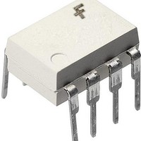
FOD3184 Fairchild Semiconductor, FOD3184 Datasheet - Page 3

FOD3184
Manufacturer Part Number
FOD3184
Description
MOSFET & Power Driver ICs 3A High Speed MOSFET Gate Driver Opto
Manufacturer
Fairchild Semiconductor
Type
High Speed MOSFET/IGBT Gate Driver Optocouplerr
Datasheet
1.FOD3184.pdf
(23 pages)
Specifications of FOD3184
Product
MOSFET Gate Drivers
Rise Time
27 ns
Fall Time
20 ns
Propagation Delay Time
145 ns
Supply Voltage (max)
35 V
Supply Voltage (min)
- 0.5 V
Supply Current
25 mA
Maximum Power Dissipation
295 mW
Maximum Operating Temperature
+ 100 C
Mounting Style
Through Hole
Maximum Turn-off Delay Time
0.3 us
Maximum Turn-on Delay Time
2 us
Minimum Operating Temperature
- 40 C
Number Of Drivers
1
Number Of Outputs
2
Output Current
3 A
Output Voltage
30 V
Package / Case
DIP-8
Number Of Elements
1
Input Type
DC
Output Type
Push-Pull
Forward Voltage
1.8V
Forward Current
25mA
Isolation Voltage
5000Vrms
Operating Temp Range
-40C to 100C
Power Dissipation
295mW
Pin Count
8
Mounting
Through Hole
Reverse Breakdown Voltage
5V
Operating Temperature Classification
Industrial
Lead Free Status / RoHS Status
Lead free / RoHS Compliant
Available stocks
Company
Part Number
Manufacturer
Quantity
Price
Part Number:
FOD3184
Manufacturer:
FAIRCHILD/ن»™ç«¥
Quantity:
20 000
©2005 Fairchild Semiconductor Corporation
FOD3184 Rev. 1.0.4
Safety and Insulation Ratings
As per DIN EN/IEC 60747-5-2. This optocoupler is suitable for “safe electrical insulation” only within the safety
limit data. Compliance with the safety ratings shall be ensured by means of protective circuits.
P
Symbol
I
S,OUTPUT
S,INPUT
V
V
T
V
CTI
R
IORM
IOTM
Case
PR
IO
Installation Classifications per DIN VDE 0110/1.89 Table 1
Climatic Classification
Pollution Degree (DIN VDE 0110/1.89)
Comparative Tracking Index
Input to Output Test Voltage, Method b,
V
tm = 1 sec., Partial Discharge < 5pC
Input to Output Test Voltage, Method a,
V
tm = 60 sec.,Partial Discharge < 5 pC
Max Working Insulation Voltage
Highest Allowable Over Voltage
External Creepage
External Clearance
External Clearance (for Option T or TS - 0.4” Lead Spacing)
Insulation Thickness
Safety Limit Values – Maximum Values Allowed in the
Event of a Failure
Insulation Resistance at T
IORM
IORM
For Rated Mains Voltage < 150Vrms
For Rated Mains Voltage < 300Vrms
For Rated Mains Voltage < 450Vrms
For Rated Mains Voltage < 600Vrms
For Rated Mains Voltage < 1000Vrms (Option T, TS)
Case Temperature
Input Current
Output Power
x 1.875 = V
x 1.5 = V
PR
PR
, Type and Sample Test with
, 100% Production Test with
Parameter
S
, V
IO
= 500V
3
1,414
10.16
Min.
2651
2121
6000
175
150
250
10
7.4
0.5
25
8
9
40/100/21
Typ.
I–IV
I–IV
I–III
I–III
I–III
2
Max.
www.fairchildsemi.com
V
V
Unit
mW
mm
mm
mm
mm
mA
°C
peak
peak
Ω


