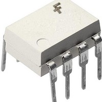
FOD3184 Fairchild Semiconductor, FOD3184 Datasheet - Page 7

FOD3184
Manufacturer Part Number
FOD3184
Description
MOSFET & Power Driver ICs 3A High Speed MOSFET Gate Driver Opto
Manufacturer
Fairchild Semiconductor
Type
High Speed MOSFET/IGBT Gate Driver Optocouplerr
Datasheet
1.FOD3184.pdf
(23 pages)
Specifications of FOD3184
Product
MOSFET Gate Drivers
Rise Time
27 ns
Fall Time
20 ns
Propagation Delay Time
145 ns
Supply Voltage (max)
35 V
Supply Voltage (min)
- 0.5 V
Supply Current
25 mA
Maximum Power Dissipation
295 mW
Maximum Operating Temperature
+ 100 C
Mounting Style
Through Hole
Maximum Turn-off Delay Time
0.3 us
Maximum Turn-on Delay Time
2 us
Minimum Operating Temperature
- 40 C
Number Of Drivers
1
Number Of Outputs
2
Output Current
3 A
Output Voltage
30 V
Package / Case
DIP-8
Number Of Elements
1
Input Type
DC
Output Type
Push-Pull
Forward Voltage
1.8V
Forward Current
25mA
Isolation Voltage
5000Vrms
Operating Temp Range
-40C to 100C
Power Dissipation
295mW
Pin Count
8
Mounting
Through Hole
Reverse Breakdown Voltage
5V
Operating Temperature Classification
Industrial
Lead Free Status / RoHS Status
Lead free / RoHS Compliant
Available stocks
Company
Part Number
Manufacturer
Quantity
Price
Part Number:
FOD3184
Manufacturer:
FAIRCHILD/ن»™ç«¥
Quantity:
20 000
©2005 Fairchild Semiconductor Corporation
FOD3184 Rev. 1.0.4
Notes:
1. Derate linearly above +79°C free air temperature at a rate of 0.37mA/°C.
2. Maximum pulse width = 10µs.
3
4. In this test, V
5. Maximum pulse width = 1ms, maximum duty cycle = 20%.
6. t
7. PWD is defined as | t
8. The difference between t
9. Pin 1 and 4 need to be connected to LED common.
10. Common mode transient immunity in the high state is the maximum tolerable dV
11. Common mode transient immunity in a low state is the maximum tolerable dV
12. In accordance with UL 1577, each optocoupler is proof tested by applying an insulation test voltage > 6000Vrms,
13. Device considered a two-terminal device: pins on input side shorted together and pins on output side shorted
Derate linearly above +79°C, free air temperature at the rate of 5.73mW/°C.
as I
falling edge of the V
pulse to the 50% level of the rising edge of the V
equal loads.
V
V
60Hz for 1 second (leakage detection current limit I
together.
PHL
CM
CM
OH
, to assure that the output will remain in a low state (i.e. V
propagation delay is measured from the 50% level on the falling edge of the input pulse to the 50% level of the
to assure that the output will remain in the high state (i.e. V
approaches zero amps.
OH
is measured with a dc load current of 100mA. When driving capacitive load V
O
PHL
signal. t
PHL
– t
PLH
and t
PLH
| for any given device.
propagation delay is measured from the 50% level on the rising edge of the input
PLH
between any two FOD3184 parts under same operating conditions, with
O
signal.
I-O
< 10µA).
7
O
< 1.0V).
O
> 15V).
CM
CM
/dt of the common mode pulse,
/dt of the common mode pulse
OH
will approach V
www.fairchildsemi.com
DD


