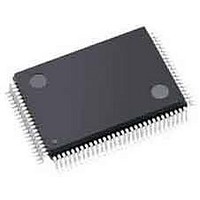
LC4064V-75TN100C Lattice, LC4064V-75TN100C Datasheet - Page 11

LC4064V-75TN100C
Manufacturer Part Number
LC4064V-75TN100C
Description
CPLD - Complex Programmable Logic Devices PROGRAMMABLE SUPER FAST HI DENSITY PLD
Manufacturer
Lattice
Series
ispMACH®r
Datasheet
1.LC4256V-75TN100I.pdf
(94 pages)
Specifications of LC4064V-75TN100C
Memory Type
EEPROM
Number Of Macrocells
64
Number Of Product Terms Per Macro
80
Maximum Operating Frequency
400 MHz
Delay Time
2.5 ns
Number Of Programmable I/os
388
Operating Supply Voltage
3.3 V
Supply Current
12 mA
Maximum Operating Temperature
+ 90 C
Minimum Operating Temperature
0 C
Package / Case
TQFP-100
Mounting Style
SMD/SMT
Supply Voltage (max)
3.6 V
Supply Voltage (min)
3 V
Programmable Type
CPLD
Voltage - Input
3 V ~ 3.6 V
Speed
7.5ns
Mounting Type
*
Lead Free Status / RoHS Status
Lead free / RoHS Compliant
Available stocks
Company
Part Number
Manufacturer
Quantity
Price
Company:
Part Number:
LC4064V-75TN100C
Manufacturer:
LATTICE
Quantity:
1 831
Company:
Part Number:
LC4064V-75TN100C
Manufacturer:
LATTICE43
Quantity:
330
Company:
Part Number:
LC4064V-75TN100C
Manufacturer:
Lattice Semiconductor Corporation
Quantity:
10 000
Part Number:
LC4064V-75TN100C
Manufacturer:
LATTICE
Quantity:
20 000
Part Number:
LC4064V-75TN100C-10I
Manufacturer:
LATTICE
Quantity:
20 000
Lattice Semiconductor
Table 10. ORP Combinations for I/O Blocks with 12 I/Os
ORP Bypass and Fast Output Multiplexers
The ORP bypass and fast-path output multiplexer is a 4:1 multiplexer and allows the 5-PT fast path to bypass the
ORP and be connected directly to the pin with either the regular output or the inverted output. This multiplexer also
allows the register output to bypass the ORP to achieve faster t
Output Enable Routing Multiplexers
The OE Routing Pool provides the corresponding local output enable (OE) product term to the I/O cell.
I/O Cell
The I/O cell contains the following programmable elements: output buffer, input buffer, OE multiplexer and bus
maintenance circuitry. Figure 8 details the I/O cell.
Figure 8. I/O Cell
Each output supports a variety of output standards dependent on the V
also be configured for open drain operation. Each input can be programmed to support a variety of standards, inde-
pendent of the V
I/O Cell
I/O 10
I/O 11
I/O 0
I/O 1
I/O 2
I/O 3
I/O 4
I/O 5
I/O 6
I/O 7
I/O 8
I/O 9
CCO
From ORP
supplied to its I/O bank. The I/O standards supported are:
M0, M1, M2, M3, M4, M5, M6, M7
M1, M2, M3, M4, M5, M6, M7, M8
M2, M3, M4, M5, M6, M7, M8, M9
M4, M5, M6, M7, M8, M9, M10, M11
M5, M6, M7, M8, M9, M10, M11, M12
M6, M7, M8, M9, M10, M11, M12, M13
M8, M9, M10, M11, M12, M13, M14, M15
M9, M10, M11, M12, M13, M14, M15, M0
M10, M11, M12, M13, M14, M15, M0, M1
M12, M13, M14, M15, M0, M1, M2, M3
M13, M14, M15, M0, M1, M2, M3, M4
M14, M15, M0, M1, M2, M3, M4, M5
GOE 0
GOE 1
GOE 2
GOE 3
VCC
To Macrocell
From ORP
To GRP
11
Available Macrocells
ispMACH 4000V/B/C/Z Family Data Sheet
CO
.
V
CCO
CCO
*Global fuses
supplied to its I/O bank. Outputs can
V
CCO
*
*
*


