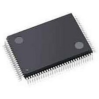
LC4064V-75TN100C Lattice, LC4064V-75TN100C Datasheet - Page 12

LC4064V-75TN100C
Manufacturer Part Number
LC4064V-75TN100C
Description
CPLD - Complex Programmable Logic Devices PROGRAMMABLE SUPER FAST HI DENSITY PLD
Manufacturer
Lattice
Series
ispMACH®r
Datasheet
1.LC4256V-75TN100I.pdf
(94 pages)
Specifications of LC4064V-75TN100C
Memory Type
EEPROM
Number Of Macrocells
64
Number Of Product Terms Per Macro
80
Maximum Operating Frequency
400 MHz
Delay Time
2.5 ns
Number Of Programmable I/os
388
Operating Supply Voltage
3.3 V
Supply Current
12 mA
Maximum Operating Temperature
+ 90 C
Minimum Operating Temperature
0 C
Package / Case
TQFP-100
Mounting Style
SMD/SMT
Supply Voltage (max)
3.6 V
Supply Voltage (min)
3 V
Programmable Type
CPLD
Voltage - Input
3 V ~ 3.6 V
Speed
7.5ns
Mounting Type
*
Lead Free Status / RoHS Status
Lead free / RoHS Compliant
Available stocks
Company
Part Number
Manufacturer
Quantity
Price
Company:
Part Number:
LC4064V-75TN100C
Manufacturer:
LATTICE
Quantity:
1 831
Company:
Part Number:
LC4064V-75TN100C
Manufacturer:
LATTICE43
Quantity:
330
Company:
Part Number:
LC4064V-75TN100C
Manufacturer:
Lattice Semiconductor Corporation
Quantity:
10 000
Part Number:
LC4064V-75TN100C
Manufacturer:
LATTICE
Quantity:
20 000
Part Number:
LC4064V-75TN100C-10I
Manufacturer:
LATTICE
Quantity:
20 000
Lattice Semiconductor
All of the I/Os and dedicated inputs have the capability to provide a bus-keeper latch, Pull-up Resistor or Pull-down
Resistor. A fourth option is to provide none of these. The selection is done on a global basis. The default in both
hardware and software is such that when the device is erased or if the user does not specify, the input structure is
configured to be a Pull-up Resistor.
Each ispMACH 4000 device I/O has an individually programmable output slew rate control bit. Each output can be
individually configured for fast slew or slow slew. The typical edge rate difference between fast and slow slew set-
ting is 20%. For high-speed designs with long, unterminated traces, the slow-slew rate will introduce fewer reflec-
tions, less noise and keep ground bounce to a minimum. For designs with short traces or well terminated lines, the
fast slew rate can be used to achieve the highest speed.
Global OE Generation
Most ispMACH 4000 family devices have a 4-bit wide Global OE Bus, except the ispMACH 4032 device that has a
2-bit wide Global OE Bus. This bus is derived from a 4-bit internal global OE PT bus and two dual purpose I/O or
GOE pins. Each signal that drives the bus can optionally be inverted.
Each GLB has a block-level OE PT that connects to all bits of the Global OE PT bus with four fuses. Hence, for a
256-macrocell device (with 16 blocks), each line of the bus is driven from 16 OE product terms. Figures 9 and 10
show a graphical representation of the global OE generation.
Figure 9. Global OE Generation for All Devices Except ispMACH 4032
• LVTTL
• LVCMOS 3.3
• LVCMOS 2.5
Shared PTOE
(Block 0)
Shared PTOE
(Block n)
• LVCMOS 1.8
• 3.3V PCI Compatible
Internal Global OE
Fuse connection
Hard wired
(4 lines)
PT Bus
Global OE
12
ispMACH 4000V/B/C/Z Family Data Sheet
Global
Fuses
Global OE Bus
to I/O cells
GOE (0:3)
4-Bit


