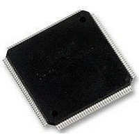
LFXP3C-4TN144C Lattice, LFXP3C-4TN144C Datasheet - Page 170

LFXP3C-4TN144C
Manufacturer Part Number
LFXP3C-4TN144C
Description
FPGA - Field Programmable Gate Array 3.1K LUTs 100 I/O 1.8/2.5/3.3V -4 Spd
Manufacturer
Lattice
Specifications of LFXP3C-4TN144C
Number Of Programmable I/os
100
Data Ram Size
55296
Supply Voltage (max)
3.465 V
Maximum Operating Temperature
+ 85 C
Minimum Operating Temperature
0 C
Mounting Style
SMD/SMT
Supply Voltage (min)
1.71 V
Package / Case
TQFP-144
Lead Free Status / RoHS Status
Lead free / RoHS Compliant
Available stocks
Company
Part Number
Manufacturer
Quantity
Price
Company:
Part Number:
LFXP3C-4TN144C
Manufacturer:
Lattice
Quantity:
135
Company:
Part Number:
LFXP3C-4TN144C
Manufacturer:
Lattice Semiconductor Corporation
Quantity:
10 000
Company:
Part Number:
LFXP3C-4TN144C-3I
Manufacturer:
TI
Quantity:
19
- Current page: 170 of 397
- Download datasheet (10Mb)
Memory Usage Guide
Lattice Semiconductor
LatticeECP/EC and LatticeXP Devices
Figure 9-5. Example Generating Pseudo Dual Port RAM (RAM_DP) Using IPexpress
In the right-hand pane, options like Macro Type, Version, and Module_Name are device and selected module
dependent. These cannot be changed in IPexpress.
Users can change the directory where the generated module files will be placed by clicking the browse button in
the Project Path.
The File Name text box allows users to specify the entity and file name for the module they are about to generate.
Users must provide this name.
Design Entry, Verilog or VHDL, by default is the same as the project type. If the project is a VHDL project, the
selected Design Entry option will be “Schematic/ VHDL”, and “Schematic/ Verilog-HDL” if the project type is Verilog-
HDL.
Then click the Customize button. This opens another window where the RAM can be customized.
The the left-hand side of this window shows the block diagram of the module. The right-hand side includes the
Configuration tab.
9-5
Related parts for LFXP3C-4TN144C
Image
Part Number
Description
Manufacturer
Datasheet
Request
R

Part Number:
Description:
FPGA - Field Programmable Gate Array 3.1K LUTs 62 I/O 1.8/2.5/3.3V -4 Spd
Manufacturer:
Lattice
Datasheet:

Part Number:
Description:
FPGA - Field Programmable Gate Array 3.1K LUTs 136 IO 1.8 /2.5/3.3V -4 Spd
Manufacturer:
Lattice

Part Number:
Description:
FPGA - Field Programmable Gate Array 3.1K LUTs 100 IO 1.8 /2.5/3.3V -4 Spd I
Manufacturer:
Lattice

Part Number:
Description:
FPGA - Field Programmable Gate Array 3.1K LUTs 136 IO 1.8 /2.5/3.3V -4 Spd I
Manufacturer:
Lattice

Part Number:
Description:
FPGA - Field Programmable Gate Array 3.1K LUTS 100 I/O
Manufacturer:
Lattice
Datasheet:

Part Number:
Description:
FPGA - Field Programmable Gate Array 3.1K LUTS 136 I/O
Manufacturer:
Lattice
Datasheet:

Part Number:
Description:
FPGA - Field Programmable Gate Array 3.1K LUTS 62 I/O
Manufacturer:
Lattice
Datasheet:

Part Number:
Description:
FPGA - Field Programmable Gate Array 3.1K LUTS 62 I/O
Manufacturer:
Lattice
Datasheet:

Part Number:
Description:
FPGA - Field Programmable Gate Array 3.1K LUTs 62 IO 1.8/ 2.5/3.3V -3 Spd I
Manufacturer:
Lattice
Datasheet:

Part Number:
Description:
FPGA - Field Programmable Gate Array 3.1K LUTs 100 I/O 1.8/2.5/3.3V IND
Manufacturer:
Lattice
Datasheet:

Part Number:
Description:
FPGA, 1.8V FLASH, INSTANT ON, SMD
Manufacturer:
LATTICE SEMICONDUCTOR
Datasheet:
Part Number:
Description:
FPGA LatticeXP Family 3000 Cells 320MHz 130nm (CMOS) Technology 1.8V/2.5V/3.3V 208-Pin PQFP Tray
Manufacturer:
LATTICE SEMICONDUCTOR
Datasheet:
Part Number:
Description:
FPGA LatticeXP Family 3000 Cells 320MHz 130nm (CMOS) Technology 1.8V/2.5V/3.3V 144-Pin TQFP Tray
Manufacturer:
LATTICE SEMICONDUCTOR
Datasheet:
Part Number:
Description:
FPGA LatticeXP Family 3000 Cells 360MHz 130nm (CMOS) Technology 1.8V/2.5V/3.3V 100-Pin TQFP Tray
Manufacturer:
LATTICE SEMICONDUCTOR
Datasheet:
Part Number:
Description:
FPGA LatticeXP Family 3000 Cells 360MHz 130nm (CMOS) Technology 1.8V/2.5V/3.3V 144-Pin TQFP Tray
Manufacturer:
LATTICE SEMICONDUCTOR
Datasheet:


