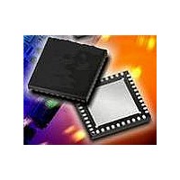
MAX2059ETL+ Maxim Integrated Products, MAX2059ETL+ Datasheet - Page 11

MAX2059ETL+
Manufacturer Part Number
MAX2059ETL+
Description
RF Mixer IC DVGA SPI HI LIN igh Linearity, SPI-C
Manufacturer
Maxim Integrated Products
Datasheet
1.MAX2059ETL.pdf
(14 pages)
Specifications of MAX2059ETL+
Lead Free Status / RoHS Status
Lead free / RoHS Compliant
The MAX2059 high-linearity DVGA consists of two 5-bit
digital attenuators, a fixed-gain two-stage driver amplifi-
er, a loopback mixer, and a serial interface to control
the attenuators. This high level of component integra-
tion makes the MAX2059 ideal for base-station trans-
mitter applications. The MAX2059 is designed to
operate in the 1700MHz to 2200MHz frequency range.
The overall cascaded performance of the MAX2059
produces a typical 10.9dB gain, a +31.8dBm OIP3, an
18.4dBm OP1dB, and a total 56dB gain-control range.
The MAX2059 integrates two 5-bit digital attenuators to
achieve a high dynamic range. Each attenuator is pro-
grammed with a 3-wire SPI interface, with a total effec-
tive range of 28dB and step size of 1dB. See the
Applications Information section and Table 1 for attenu-
ator programming details. The attenuators can be used
for both static and dynamic power control.
Table 1. Attenuator Programming
Note: Due to finite circuit isolation, the total effective range of
each attenuator is limited to 28dB.
Figure 1. SPI Timing Diagram
CLOCK
DATA
ATTENUATOR A (5 MSBs)
SPI-Controlled DVGA with Integrated Loopback Mixer
CS
MSB
NOTES:
DATA ENTERED ON CLOCK RISING EDGE.
ATTENUATOR STATE CHANGE ON CS RISING EDGE.
Bit 9 = 16dB step
Bit 8 = 8dB step
Bit 7 = 4dB step
Bit 6 = 2dB step
Bit 5 = 1dB step
BIT 9
BIT 8
t
CS
______________________________________________________________________________________
Detailed Description
t
EWN
ATTENUATOR B (5 LSBs)
5-Bit Attenuators
Bit 4 = 16dB step
Bit 3 = 8dB step
Bit 2 = 4dB step
Bit 1 = 2dB step
Bit 0 = 1dB step
BIT 1
t
CH
1700MHz to 2200MHz High-Linearity,
BIT 0
t
CW
t
ES
LSB
t
EW
The MAX2059 includes a two-stage medium power
amplifier with a fixed 18.5dB gain. The driver amplifier
circuit is optimized for high linearity and medium output
power capability for the 1800MHz to 2000MHz frequen-
cy range. The driver amplifier is intended to amplify a
modulated signal and drive a high-power amplifier in
base-station transmitters. In a typical application, the
driver amplifier is cascaded in between the two digital
attenuators. See the Typical Application Circuit.
The two-stage amplifier stage can be disabled for
applications where only the digital attenuators and/or
loopback mixer are used. To disable the two-stage
amplifier, ground or leave unconnected the amplifier
supplies VCCBIAS2, VCCAMP, VCCBIAS1, and also
the inputs for setting the amplifier bias currents RSET1,
RSET2. This reduces the supply current by approxi-
mately 187mA under typical conditions.
The MAX2059 loopback mixer uses a double-balanced
active architecture designed to operate with a
1700MHz to 2200MHz RF frequency range, and a
40MHz to 100MHz LO frequency range. The RF port of
the mixer is connected internally (with an on-chip
switch) to the input of the first attenuator stage. The
mixer’s IF port is matched for a single-ended 50Ω
impedance, while the LO port requires a differential
input impedance of 100Ω.
The loopback mixer facilitates a self-diagnostic mode
for cellular transceivers, whereby the Tx band signal at
the input of the mixer can be translated up or down to
the corresponding Rx band. This translated signal can
then be fed back to the radio’s receiver for complete
Tx/Rx loop diagnostics. The loopback mixer is enabled
and disabled with LB_EN. Set LB_EN to a logic-low 0 to
enable the mixer, set LB_EN to a logic-high 1 to disable
the mixer.
The MAX2059 loopback mixer accepts a nominal -6dBm
LO input power and exhibits a -12.6dBm output power
and an output IP3 of 6.2dBm (P
The two 5-bit attenuators are programmed with the 3-
wire SPI/MICROWIRE-compatible serial interface using
10-bit words. Bit 9 of the 10-bit data is shifted in first,
along with all remaining data bits, on the rising edge of
the clock regardless of CS being high or low. Once all
the data bits are shifted in, all will be sent to the attenua-
tors on the rising edge of CS, thus changing the attenua-
tion state. For standard SPI operation, pull CS low for the
SPI Interface and Attenuator Settings
Applications Information
IN
= +5dBm).
Loopback Mixer
Driver Amplifier
11


