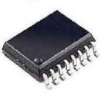
DG403DY-E3 Vishay, DG403DY-E3 Datasheet - Page 9

DG403DY-E3
Manufacturer Part Number
DG403DY-E3
Description
Analog Switch ICs SPDT Analog Switch
Manufacturer
Vishay
Type
Analog Switchr
Datasheet
1.DG403DY-T1-E3.pdf
(12 pages)
Specifications of DG403DY-E3
Number Of Switches
Dual
Switch Configuration
SPDT
On Resistance (max)
45 Ohms @ +/- 13.5 V
On Time (max)
150 ns @ +/- 15 V
Off Time (max)
100 ns @ +/- 15 V
Supply Voltage (max)
25 V
Supply Current
0.00001 mA @ +/- 16.5 V
Maximum Power Dissipation
600 mW
Maximum Operating Temperature
+ 85 C
Mounting Style
SMD/SMT
Package / Case
SOIC-16 Narrow
Minimum Operating Temperature
- 40 C
Analog Switch Type
SPDT
No. Of Channels
2
On State Resistance Max
30ohm
Turn Off Time
30ns
Turn On Time
75ns
Supply Voltage Range
± 15V
Operating Temperature Range
-40°C To +85°C
Package
16SOIC N
Maximum On Resistance
55@±13.5V Ohm
Maximum High Level Output Current
100 mA
Number Of Channels Per Chip
2
Maximum Turn-off Time
100@±15V ns
Maximum Turn-on Time
150@±15V ns
Switch Architecture
SPDT
Power Supply Type
Single|Dual
Multiplexer Configuration
Dual SPDT
Number Of Inputs
4
Number Of Outputs
4
Number Of Channels
2
Analog Switch On Resistance
45@±13.5VOhm
Package Type
SOIC N
Power Supply Requirement
Single/Dual
Single Supply Voltage (min)
13V
Single Supply Voltage (typ)
15/18/24/28V
Single Supply Voltage (max)
36V
Dual Supply Voltage (min)
±7V
Dual Supply Voltage (typ)
±9/±12/±15/±18V
Dual Supply Voltage (max)
±22V
Power Dissipation
600mW
Mounting
Surface Mount
Pin Count
16
Operating Temp Range
-40C to 85C
Operating Temperature Classification
Industrial
Lead Free Status / RoHS Status
Lead free / RoHS Compliant
Lead Free Status / RoHS Status
Lead free / RoHS Compliant, Lead free / RoHS Compliant
TEST CIRCUITS
Document Number: 70049
S09-2561-Rev. I, 30-Nov-09
V
V
S
S
R
R
g
g
0 V, 2.4 V
C = RF bypass
= 50
= 50
0 V, 2.4 V
Ω
Ω
Figure 6. Insertion Loss
Figure 5. Off Isolation
C
C
S
IN
S
IN
C = RF bypass
GND
+ 5 V
GND
Off Isolation = 20 log
+ 5 V
V
V
L
L
+ 15 V
+ 15 V
- 15 V
- 15 V
V+
V-
V-
V+
D
D
C
V
V
C
C
S
O
C
R
100
R
100
V
L
V
O
L
O
Ω
Ω
0 V, 2.4 V
V
S
V
R
R
O
g
L
= 50
C
Ω
IN
0.8 V
+ 5 V
GND
V
DG401, DG403, DG405
L
C = RF bypass
C
Figure 8. Capacitances
Figure 7. Crosstalk
X
TALK
S
S
IN
+ 5 V
1
2
GND
+ 15 V
- 15 V
V
V-
L
Isolation = 20 log
V+
S
D
Vishay Siliconix
C
C
+ 15 V
- 15 V
V+
V-
D
V
V
www.vishay.com
S
O
or Equivalent
Impedance
C
C
HP4192A
f = 1 MHz
Analyzer
Meter
50
Ω
9


