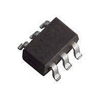
IP4233CZ6,125 NXP Semiconductors, IP4233CZ6,125 Datasheet

IP4233CZ6,125
Specifications of IP4233CZ6,125
Available stocks
Related parts for IP4233CZ6,125
IP4233CZ6,125 Summary of contents
Page 1
IP4233CZ6 Ultra low capacitance ESD protection for Ethernet ports Rev. 3 — 17 June 2010 1. Product profile 1.1 General description The IP4233CZ6 is designed to protect Input/Output (I/O) ports that are sensitive to capacitive loads, such as Ethernet, from ...
Page 2
... NXP Semiconductors 2. Pinning information Table 2. Pin Ordering information Table 3. Type number IP4233CZ6 4. Limiting values Table 4. In accordance with the Absolute Maximum Rating System (IEC 60134). Symbol ESD T stg T amb 5. Characteristics Table 5. ° unless otherwise specified. amb Symbol C (I/O-GND [1] Guaranteed by design. [2] Pins and pins ...
Page 3
... NXP Semiconductors 6. Application information A typical application for protecting a 10/100 Mbit/s Ethernet transceiver against ESD is shown in Figure 10/100 BASE-T ETHERNET Fig 1. Typical application for ESD protection of a 10/100 Mbit/s Ethernet transceiver IP4233CZ6 Product data sheet Ultra low capacitance ESD protection for Ethernet ports 1 ...
Page 4
... NXP Semiconductors 7. Package outline Plastic surface-mounted package; 6 leads pin 1 index DIMENSIONS (mm are the original dimensions UNIT max 0.30 1.1 0.25 mm 0.1 0.20 0.8 0.10 OUTLINE VERSION IEC SOT363 Fig 2. Package outline SOT363 (SC-88) IP4233CZ6 Product data sheet Ultra low capacitance ESD protection for Ethernet ports ...
Page 5
... NXP Semiconductors 8. Soldering of SMD packages This text provides a very brief insight into a complex technology. A more in-depth account of soldering ICs can be found in Application Note AN10365 “Surface mount reflow soldering description”. 8.1 Introduction to soldering Soldering is one of the most common methods through which packages are attached to Printed Circuit Boards (PCBs), to form electrical circuits ...
Page 6
... NXP Semiconductors 8.4 Reflow soldering Key characteristics in reflow soldering are: • Lead-free versus SnPb soldering; note that a lead-free reflow process usually leads to higher minimum peak temperatures (see reducing the process window • Solder paste printing issues including smearing, release, and adjusting the process window for a mix of large and small components on one board • ...
Page 7
... NXP Semiconductors temperature MSL: Moisture Sensitivity Level Fig 3. Temperature profiles for large and small components For further information on temperature profiles, refer to Application Note AN10365 “Surface mount reflow soldering description”. IP4233CZ6 Product data sheet Ultra low capacitance ESD protection for Ethernet ports ...
Page 8
... NXP Semiconductors 9. Revision history Table 8. Revision history Document ID Release date IP4233CZ6 v.3 20100617 • Modifications: Figure • Section 10 “Legal IP4233CZ6 v.2 20100506 IP4233CZ6_1 20090330 IP4233CZ6 Product data sheet Ultra low capacitance ESD protection for Ethernet ports Data sheet status Product data sheet 1: corrected information” ...
Page 9
... In no event shall NXP Semiconductors be liable for any indirect, incidental, punitive, special or consequential damages (including - without limitation - lost profits, lost savings, business interruption, costs related to the removal or ...
Page 10
... NXP Semiconductors’ specifications such use shall be solely at customer’s own risk, and (c) customer fully indemnifies NXP Semiconductors for any liability, damages or failed product claims resulting from customer design and use of the product for automotive applications beyond NXP Semiconductors’ ...
Page 11
... NXP Semiconductors 12. Contents 1 Product profile . . . . . . . . . . . . . . . . . . . . . . . . . . 1 1.1 General description . . . . . . . . . . . . . . . . . . . . . 1 1.2 Features and benefits . . . . . . . . . . . . . . . . . . . . 1 1.3 Applications . . . . . . . . . . . . . . . . . . . . . . . . . . . 1 1.4 Quick reference data . . . . . . . . . . . . . . . . . . . . 1 2 Pinning information . . . . . . . . . . . . . . . . . . . . . . 2 3 Ordering information . . . . . . . . . . . . . . . . . . . . . 2 4 Limiting values Characteristics . . . . . . . . . . . . . . . . . . . . . . . . . . 2 6 Application information Package outline . . . . . . . . . . . . . . . . . . . . . . . . . 4 8 Soldering of SMD packages . . . . . . . . . . . . . . . 5 8.1 Introduction to soldering . . . . . . . . . . . . . . . . . . 5 8.2 Wave and reflow soldering ...


