MC56F8245VLD Freescale Semiconductor, MC56F8245VLD Datasheet - Page 23
MC56F8245VLD
Manufacturer Part Number
MC56F8245VLD
Description
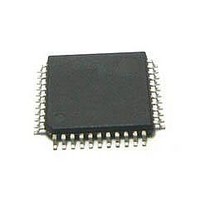
DSC 48K FLASH 60MHZ 44-LQFP
Manufacturer
Freescale Semiconductor
Series
56F8xxxr
Datasheets
1.TWR-56F8257.pdf
(88 pages)
2.MC56F8245VLD.pdf
(14 pages)
3.MC56F8245VLD.pdf
(2 pages)
4.MC56F8245VLD.pdf
(629 pages)
Specifications of MC56F8245VLD
Core Processor
56800E
Core Size
16-Bit
Speed
60MHz
Connectivity
CAN, I²C, LIN, SCI, SPI
Peripherals
LVD, POR, PWM, WDT
Number Of I /o
35
Program Memory Size
48KB (24K x 16)
Program Memory Type
FLASH
Ram Size
3K x 16
Voltage - Supply (vcc/vdd)
3 V ~ 3.6 V
Data Converters
A/D 8x12b, D/A 1x12b
Oscillator Type
Internal
Operating Temperature
-40°C ~ 105°C
Package / Case
44-LQFP
Product
DSCs
Processor Series
56800E
Core
56800E
Device Million Instructions Per Second
60 MIPs
Maximum Clock Frequency
60 MHz
Number Of Programmable I/os
35
Data Ram Size
6 KB
Operating Supply Voltage
3.3 V
Maximum Operating Temperature
+ 105 C
Mounting Style
SMD/SMT
Minimum Operating Temperature
- 40 C
On-chip Adc
12 bit, 4 Channel
Package
44LQFP
Family Name
MC56F82xx
Maximum Speed
60 MHz
Data Bus Width
16 Bit
Interface Type
I2C/SCI/SPI
On-chip Dac
1-chx12-bit
Number Of Timers
8
Lead Free Status / RoHS Status
Lead free / RoHS Compliant
Eeprom Size
-
Lead Free Status / Rohs Status
Details
Available stocks
Company
Part Number
Manufacturer
Quantity
Price
Company:

Part Number:
MC56F8245VLD
Manufacturer:
FREESCAL
Quantity:
269
Company:
Part Number:
MC56F8245VLD
Manufacturer:
Freescale Semiconductor
Quantity:
10 000


Freescale Semiconductor
(CMPB_O)
(CMPA_O)
(XB_IN2)
(XB_IN7)
GPIOC2
GPIOC3
GPIOC4
GPIOC5
(DACO)
(CLKO)
(RXD0)
(TXD0)
Signal
Name
(TB0)
(TA0)
(TA1)
LQFP
44
12
5
6
7
Table 5. MC56F825x/MC56F824x Signal and Package Information (continued)
LQFP
48
13
5
6
7
LQFP
64
18
5
7
8
MC56F825x/MC56F824x Digital Signal Controller, Rev. 3
Output
Output
Output
Output
Output
Output
Output
Output
Output
Output
Output
Analog
Output
Input/
Input/
Input/
Input/
Input/
Input/
Input/
Type
Input
Input
Input
enabled
enabled
enabled
enabled
internal
internal
internal
internal
During
Reset
pullup
pullup
pullup
pullup
Input,
Input,
Input,
Input,
State
Port C GPIO — This GPIO pin can be individually programmed as
an input or output pin.
TXD0 — The SCI0 transmit data output or transmit/receive in single
wire operation.
TB0 — Quad timer module B channel 0 input/output.
XB_IN2 — Crossbar module input 2
CLKO — This is a buffered clock output; the clock source is selected
by clockout select (CLKOSEL) bits in the clock output select register
(CLKOUT) of the SIM.
After reset, the default state is GPIOC2.
Port C GPIO — This GPIO pin can be individually programmed as
an input or output pin.
TA0 — Quad timer module A channel 0 input/output.
CMPA_O— Analog comparator A output
RXD0 — The SCI0 receive data input.
After reset, the default state is GPIOC3.
Port C GPIO — This GPIO pin can be individually programmed as
an input or output pin.
TA1 — Quad timer module A channel 1input/output
CMPB_O — Analog comparator B output
After reset, the default state is GPIOC4.
Port C GPIO — This GPIO pin can be individually programmed as
an input or output pin.
DACO — 12-bit Digital-to-Analog Controller output
XB_IN7 — Crossbar module input 7
After reset, the default state is GPIOC5.
Signal Description
Signal/Connection Descriptions
23
Related parts for MC56F8245VLD
Image
Part Number
Description
Manufacturer
Datasheet
Request
R

Part Number:
Description:
Manufacturer:
Freescale Semiconductor, Inc
Datasheet:
Part Number:
Description:
Manufacturer:
Freescale Semiconductor, Inc
Datasheet:
Part Number:
Description:
Manufacturer:
Freescale Semiconductor, Inc
Datasheet:
Part Number:
Description:
Manufacturer:
Freescale Semiconductor, Inc
Datasheet:
Part Number:
Description:
Manufacturer:
Freescale Semiconductor, Inc
Datasheet:
Part Number:
Description:
Manufacturer:
Freescale Semiconductor, Inc
Datasheet:
Part Number:
Description:
Manufacturer:
Freescale Semiconductor, Inc
Datasheet:
Part Number:
Description:
Manufacturer:
Freescale Semiconductor, Inc
Datasheet:
Part Number:
Description:
Manufacturer:
Freescale Semiconductor, Inc
Datasheet:
Part Number:
Description:
Manufacturer:
Freescale Semiconductor, Inc
Datasheet:
Part Number:
Description:
Manufacturer:
Freescale Semiconductor, Inc
Datasheet:
Part Number:
Description:
Manufacturer:
Freescale Semiconductor, Inc
Datasheet:
Part Number:
Description:
Manufacturer:
Freescale Semiconductor, Inc
Datasheet:
Part Number:
Description:
Manufacturer:
Freescale Semiconductor, Inc
Datasheet:
Part Number:
Description:
Manufacturer:
Freescale Semiconductor, Inc
Datasheet: